
Microcontrollers User manual
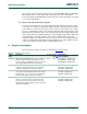


UM10237_2 © NXP B.V. 2008. All rights reserved.
User manual Rev. 02 — 19 December 2008 586 of 792
NXP Semiconductors
UM10237
Chapter 22: LPC24XX I
2
C interfaces I
2
C0/1/2
(12)
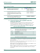
The values for I2SCLL and I2SCLH should not necessarily be the same. Software can set
different duty cycles on SCL by setting these two registers. For example, the I
2
C bus
specification defines the SCL low time and high time at different values for a 400 kHz I
2
C
rate. The value of the register must ensure that the data rate is in the I
2
C data rate range
of 0 through 400 kHz. Each register value must be greater than or equal to 4.
Table 22–520
gives some examples of I
2
C bus rates based on PCLK frequency and
I2SCLL and I2SCLH values.
9. Details of I
2
C operating modes
The four operating modes are:
• Master Transmitter
• Master Receiver
• Slave Receiver
• Slave Transmitter
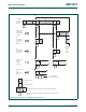
Data transfers in each mode of operation are shown in Figures 120
to 124. Table 22–521
lists abbreviations used in these figures when describing the I
2
C operating modes.
Table 520. Example I
2
C Clock Rates
I2SCLL +
I2SCLH
I
2
C Bit Frequency (kHz) at PCLK (MHz)
1 5 10 16 20 40 60
8125
10 100
25 40 200 400
50 20 100 200 320 400
100 10 50 100 160 200 400
160 6.25 31.25 62.5 100 125 250 375
200 5 25 50 80 100 200 300
400 2.5 12.5 25 40 50 100 150
800 1.256.2512.520 25 50 75
I
2
C
bitfrequency
f
PCLK
I2CSCLH I2CSCLL+
---------------------------------------------------------
=
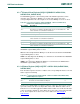
Table 521. Abbreviations used to describe an I
2
C operation
Abbreviation Explanation
S Start Condition
SLA 7 bit slave address
R Read bit (high level at SDA)
W Write bit (low level at SDA)
A Acknowledge bit (low level at SDA)