
Microcontrollers User manual


UM10237_2 © NXP B.V. 2008. All rights reserved.
User manual Rev. 02 — 19 December 2008 572 of 792
1. Basic configuration
The I
2
C0/1/2 interfaces are configured using the following registers:
1. Power: In the PCONP register (Table 4–63
), set bit PCI2C0/1/2.
Remark: On reset, all I
2
C interfaces are enabled (PCI2C0/1/2 = 1).
2. Clock: In PCLK_SEL0 select PCLK_I2C0; in PCLK_SEL1 select PCLK_I2C1/2 (see
Section 4–3.3.4
.
3. Pins: Select I
2
C pins and their modes in PINSEL0 to PINSEL4 and PINMODE0 to
PINMODE4 (see Section 9–5
).
Remark: I
2
C0 pins SDA0 and SCL0 are open-drain outputs for I
2
C-bus compliance
(see Section 9–5.14
).
4. Interrupts are enabled in the VIC using the VICIntEnable register (Table 7–106
).
5. Initialization: see Section 22–10.1
and Section 22–9.12.1.
2. Features
• Standard I
2
C compliant bus interfaces that may be configured as Master, Slave, or
Master/Slave.
• Arbitration between simultaneously transmitting masters without corruption of serial
data on the bus.
• Programmable clock to allow adjustment of I
2
C transfer rates.
• Bidirectional data transfer between masters and slaves.
• Serial clock synchronization allows devices with different bit rates to communicate via
one serial bus.
• Serial clock synchronization can be used as a handshake mechanism to suspend and
resume serial transfer.
• The I
2
C bus may be used for test and diagnostic purposes.
3. Applications
Interfaces to external I
2
C standard parts, such as serial RAMs, LCDs, tone generators,
etc.
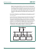
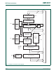
4. Description
A typical I
2
C bus configuration is shown in Figure 22–111. Depending on the state of the
direction bit (R/W), two types of data transfers are possible on the I
2
C bus:
• Data transfer from a master transmitter to a slave receiver. The first byte transmitted
by the master is the slave address. Next follows a number of data bytes. The slave
returns an acknowledge bit after each received byte.
UM10237
Chapter 22: LPC24XX I
2
C interfaces I
2
C0/1/2
Rev. 02 — 19 December 2008 User manual