
Microcontrollers User manual


UM10237_2 © NXP B.V. 2008. All rights reserved.
User manual Rev. 02 — 19 December 2008 183 of 792
NXP Semiconductors
UM10237
Chapter 9: LPC24XX Pin connect
[1] See Section 9–5.11 “Pin Function Select Register 10 (PINSEL10 - 0xE002 C028)”for details on using the
ETM functionality.
5.6 Pin Function Select Register 5 (PINSEL5 - 0xE002 C014)
The PINSEL5 register controls the functions of the pins as per the settings listed in
Table 9–136
. The direction control bit in the FIO2DIR register is effective only when the
GPIO function is selected for a pin. For other functions, direction is controlled
automatically.
The bit functions in this register depend on the number of pins of each LPC2400 part. For
the 180-pin LPC2458, see Table 9–136
. For the 208-pin LPC2460/68/70/78, see
Table 9–137
.
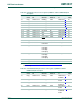
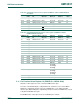
11:10 P2[5] GPIO Port 2.5 PWM1[6] DTR1 TRACEPKT0
[1]
/
LCDLP
00
13:12 P2[6] GPIO Port 2.6 PCAP1[0] RI1 TRACEPKT1
[1]
/
LCDVD[0]/
LCDVD[4]
00
15:14 P2[7] GPIO Port 2.7 RD2 RTS1 TRACEPKT2
[1]
/
LCDVD[1]/
LCDVD[5]
00
17:16 P2[8] GPIO Port 2.8 TD2 TXD2 TRACEPKT3
[1]
/
LCDVD[2]/
LCDVD[6]
00
19:18 P2[9] GPIO Port 2.9 USB_CONN
ECT1
RXD2 EXTIN0
[1]
/
LCDVD[3]/
LCDVD[7]
00
21:20 P2[10] GPIO Port 2.10 EINT0
Reserved Reserved 00
23:22 P2[11] GPIO Port 2.11 EINT1
/
LCDCLKIN
MCIDAT1 I2STX_CLK 00
25:24 P2[12] GPIO Port 2.12 EINT2
/
LCDVD[4]/
LCDVD[3]/
LCDVD[8]/
LCDVD[18]
MCIDAT2 I2STX_WS 00
27:26 P2[13] GPIO Port 2.13 EINT3
/
LCDVD[5]/
LCDVD[9]/
LCDVD[19]
MCIDAT3 I2STX_SDA 00
29:28 P2[14] GPIO Port 2.14 CS2
CAP2[0] SDA1 00
31:30 P2[15] GPIO Port 2.15 CS3
CAP2[1] SCL1 00
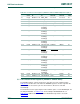
Table 135. LPC2420/60/68/70/78 pin function select register 4 (PINSEL4 - address
0xE002 C010) bit description
PINSEL4 Pin
name
Function when
00
Function
when 01
Function
when 10
Function when
11
Reset
value