
Microcontrollers User manual


UM10237_2 © NXP B.V. 2008. All rights reserved.
User manual Rev. 02 — 19 December 2008 180 of 792
NXP Semiconductors
UM10237
Chapter 9: LPC24XX Pin connect
[1] Pins P027] and P0[28] are open-drain for I
2
C0 and GPIO functionality for I
2
C-bus compliance.
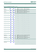
5.3 Pin Function Select register 2 (PINSEL2 - 0xE002 C008)
The PINSEL2 register controls the functions of the pins as per the settings listed in
Table 9–132
. The direction control bit in the IO1DIR register (or the FIO1DIR register if the
enhanced GPIO function is selected for port 1) is effective only when the GPIO function is
selected for a pin. For other functions, direction is controlled automatically.
5.4 Pin Function Select Register 3 (PINSEL3 - 0xE002 C00C)
The PINSEL3 register controls the functions of the pins as per the settings listed in
Table 9–133
. The direction control bit in the IO1DIR register (or the FIO1DIR register if the
enhanced GPIO function is selected for port 1) is effective only when the GPIO function is
selected for a pin. For other functions, direction is controlled automatically.
LCD functions are available in LPC2470/78 only and are selected in Table 9–145
.
27:26 P0[29] GPIO Port 0.29 USB_D+1 Reserved Reserved 00
29:28 P0[30] GPIO Port 0.30 USB_D−1 Reserved Reserved 00
31:30 P0[31] GPIO Port 0.31 USB_D+2 Reserved Reserved 00
Table 131. Pin function select register 1 (PINSEL1 - address 0xE002 C004) bit description
PINSEL1 Pin
name
Function when
00
Function
when 01
Function
when 10
Function
when 11
Reset
value
Table 132. Pin function select register 2 (PINSEL2 - address 0xE002 C008) bit description
PINSEL2 Pin
name
Function when
00
Function when
01
Function
when 10
Function
when 11
Reset
value
1:0 P1[0] GPIO Port 1.0 ENET_TXD0 Reserved Reserved 00
3:2 P1[1] GPIO Port 1.1 ENET_TXD1 Reserved Reserved 00
5:4 P1[2] GPIO Port 1.2 ENET_TXD2 MCICLK PWM0[1] 00
7:6 P1[3] GPIO Port 1.3 ENET_TXD3 MCICMD PWM0[2] 00
9:8 P1[4] GPIO Port 1.4 ENET_TX_EN Reserved Reserved 00
11:10 P1[5] GPIO Port 1.5 ENET_TX_ER MCIPWR PWM0[3] 00
13:12 P1[6] GPIO Port 1.6 ENET_TX_CLK MCIDAT0 PWM0[4] 00
15:14 P1[7] GPIO Port 1.7 ENET_COL MCIDAT1 PWM0[5] 00
17:16 P1[8] GPIO Port 1.8 ENET_CRS_DV/
ENET_CRS
Reserved Reserved 00
19:18 P1[9] GPIO Port 1.9 ENET_RXD0 Reserved Reserved 00
21:20 P1[10] GPIO Port 1.10 ENET_RXD1 Reserved Reserved 00
23:22 P1[11] GPIO Port 1.11 ENET_RXD2 MCIDAT2 PWM0[6] 00
25:24 P1[12] GPIO Port 1.12 ENET_RXD3 MACIDAT3 PCAP0[0]
27:26 P1[13] GPIO Port 1.13 ENET_RX_DV Reserved Reserved 00
29:28 P1[14] GPIO Port 1.14 ENET_RX_ER Reserved Reserved 00
31:30 P1[15] GPIO Port 1.15 ENET_REF_CLK
/ENET_RX_CLK
Reserved Reserved 00