
Microcontrollers User manual


UM10237_2 © NXP B.V. 2008. All rights reserved.
User manual Rev. 02 — 19 December 2008 173 of 792
NXP Semiconductors
UM10237
Chapter 8: LPC24XX Pin configuration
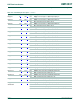
TMS 6
[1]
E3
[1]
I TMS — Test Mode Select for JTAG interface.
TRST
8
[1]
D1
[1]
I TRST — Test Reset for JTAG interface.
TCK 10
[1]
E2
[1]
I TCK — Test Clock for JTAG interface. This clock must be slower than
1
⁄
6
of the CPU clock (CCLK) for the JTAG interface to operate.
RTCK 206
[1]
C3
[1]
I/O RTCK — JTAG interface control signal.
Note: LOW on this pin while RESET is LOW enables ETM pins (P2[9:0])
to operate as Trace port after reset.
RSTOUT
29 K3 O RSTOUT — This is a 3.3 V pin. LOW on this pin indicates UM10237
being in Reset state.
RESET
35
[7]
M2
[7]
I external reset input: A LOW on this pin resets the device, causing I/O
ports and peripherals to take on their default states, and processor
execution to begin at address 0. TTL with hysteresis, 5 V tolerant.
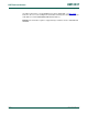
XTAL1 44
[8]
M4
[8]
I Input to the oscillator circuit and internal clock generator circuits.
XTAL2 46
[8]
N4
[8]
O Output from the oscillator amplifier.
RTCX1 34
[8]
K2
[8]
I Input to the RTC oscillator circuit.
RTCX2 36
[8]
L2
[8]
O Output from the RTC oscillator circuit.
V
SSIO
33, 63,
77, 93,
114,
133,
148,
169,
189,
200
[9]
L3, T5,
R9, P12,
N16,
H14,
E15,
A12, B6,
A2
[9]
I ground: 0 V reference for the digital IO pins.
V
SSCORE
32, 84,
172
[9]
K4, P10,
D12
[9]
I ground: 0 V reference for the core.
V
SSA
22
[10]
J2
[10]
I analog ground: 0 V reference. This should nominally be the same
voltage as V
SSIO
/V
SSCORE
, but should be isolated to minimize noise and
error.
V
DD(3V3)
15, 60,
71, 89,
112,
125,
146,
165,
181,
198
[11]
G3, P6,
P8, U13,
P17,
K16,
C17,
B13, C9,
D7
[11]
I 3.3 V supply voltage: This is the power supply voltage for the I/O ports.
n.c. 30, 117,
141
[12]
J4, L14,
G14
[12]
I not connected pins: These pins must be left unconnected (floating).
V
DD(DCDC)(3V3)
26, 86,
174
[13]
H4, P11,
D11
[13]
I 3.3 V DC-to-DC converter supply voltage: This is the power supply for
the on-chip DC-to-DC converter.
V
DDA
20
[14]
G4
[14]
I analog 3.3 V pad supply voltage: This should be nominally the same
voltage as V
DD(3V3)
but should be isolated to minimize noise and error.
This voltage is used to power the ADC and DAC.
VREF 24
[14]
K1
[14]
I ADC reference: This should be nominally the same voltage as V
DD(3V3)
but should be isolated to minimize noise and error. The level on this pin is
used as a reference for ADC and DAC.
VBAT 38
[14]
M3
[14]
I RTC power supply: 3.3 V on this pin supplies the power to the RTC
peripheral.
Table 124. LPC2470/78 pin description
…continued
Symbol Pin Ball Type Description