
Microcontrollers User manual


UM10237_2 © NXP B.V. 2008. All rights reserved.
User manual Rev. 02 — 19 December 2008 164 of 792
NXP Semiconductors
UM10237
Chapter 8: LPC24XX Pin configuration
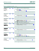
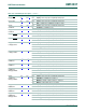
P1[29]/USB_SDA1/
LCDVD[15]/
LCDVD[23]/
PCAP1[1]/MAT0[1]
92
[1]
U14
[1]
I/O P1[29] — General purpose digital input/output pin.
I/O USB_SDA1 — USB port 1 I
2
C serial data (OTG transceiver).
[16]
O LCDVD[15]/LCDVD[23] — LCD data.
[16]
I PCAP1[1] — Capture input for PWM1, channel 1.
O MAT0[1] — Match output for Timer 0, channel 0.
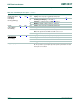
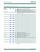
P1[30]/
USB_PWRD2/
V
BUS
/AD0[4]
42
[2]
P2
[2]
I/O P1[30] — General purpose digital input/output pin.
I USB_PWRD2 — Power Status for USB port 2.
I V
BUS
— Monitors the presence of USB bus power.
Note: This signal must be HIGH for USB reset to occur.
I AD0[4] — A/D converter 0, input 4.
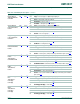
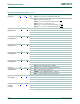
P1[31]/
USB_OVRCR2
/
SCK1/AD0[5]
40
[2]
P1
[2]
I/O P1[31] — General purpose digital input/output pin.
I USB_OVRCR2
— Over-Current status for USB port 2.
I/O SCK1 — Serial Clock for SSP1.
I AD0[5] — A/D converter 0, input 5.
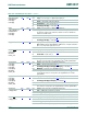
P2[0] to P2[31] I/O Port 2: Port 2 is a 32-bit I/O port with individual direction controls for each
bit. The operation of port 2 pins depends upon the pin function selected
via the pin connect block.
Table 124. LPC2470/78 pin description
…continued
Symbol Pin Ball Type Description