
Microcontrollers User manual


UM10237_2 © NXP B.V. 2008. All rights reserved.
User manual Rev. 02 — 19 December 2008 16 of 792
1. How to read this chapter
The memory addressing and mapping for different LPC2400 parts depends on flash size,
EMC size, and the LCD peripheral, see Table 2–13
.
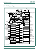
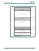
2. Memory map and peripheral addressing
ARM processors have a single 4 GB address space. The following table shows how this
space is used on NXP embedded ARM devices.
UM10237
Chapter 2: LPC24XX Memory mapping
Rev. 02 — 19 December 2008 User manual
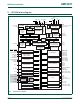
Table 13. LPC2400 memory options and addressing
Flash LCD EMC Memory map
Table 2–19;
Table 2–21
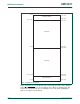
Figure 2–8
LPC2458 512 kB no 16-bit Table 2–14
LPC2420 flashless no 32-bit Table 2–15
LPC2460 flashless no 32-bit Table 2–15
LPC2468 512 kB no 32-bit Table 2–16
LPC2470 flashless yes 32-bit Table 2–15
LPC2478 512 kB yes 32-bit Table 2–16
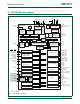
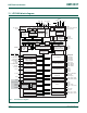
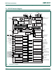
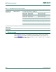
Table 14. LPC2458 memory usage and details
Address range General use Address range details and description
0x0000 0000 to
0x3FFF FFFF
On-chip non-volatile
memory and Fast I/O
0x0000 0000 - 0x0007 FFFF Flash Memory (512 kB)
0x3FFF C000 - 0x3FFF FFFF Fast GPIO registers
0x4000 0000 to
0x7FFF FFFF
On-chip RAM 0x4000 0000 - 0x4000 FFFF RAM (64 kB)
0x7FE0 0000 - 0x7FE0 3FFF Ethernet RAM (16 kB)
0x7FD0 0000 - 0x7FD0 3FFF USB RAM (16 kB)
0x8000 0000 to
0xDFFF FFFF
Off-Chip Memory Two static memory banks, 16 MB each
0x8000 0000 - 0x80FF FFFF Static memory bank 0
0x8100 0000 - 0x81FF FFFF Static memory bank 1
Two dynamic memory banks, 256 MB each
0xA000 0000 - 0xAFFF FFFF Dynamic memory bank 0
0xB000 0000 - 0xBFFF FFFF Dynamic memory bank 1
0xE000 0000 to
0xEFFF FFFF
APB Peripherals 36 peripheral blocks, 16 kB each
0xF000 0000 to
0xFFFF FFFF
AHB peripherals