
Microcontrollers User manual


UM10237_2 © NXP B.V. 2008. All rights reserved.
User manual Rev. 02 — 19 December 2008 158 of 792
NXP Semiconductors
UM10237
Chapter 8: LPC24XX Pin configuration
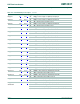
P0[4]/I2SRX_CLK/
LCDVD[0]/RD2/
CAP2[0]
168
[1]
B12
[1]
I/O P0[4] — General purpose digital input/output pin.
I/O I2SRX_CLK — I
2
S Receive clock. It is driven by the master and received
by the slave. Corresponds to the signal SCK in the I
2
S-bus
specification.
[15]
O LCDVD[0] — LCD data.
[15]
I RD2 — CAN2 receiver input.
I CAP2[0] — Capture input for Timer 2, channel 0.
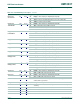
P0[5]/I2SRX_WS/
LCDVD[1]/TD2/
CAP2[1]
166
[1]
C12
[1]
I/O P0[5] — General purpose digital input/output pin.
I/O I2SRX_WS — I
2
S Receive word select. It is driven by the master and
received by the slave. Corresponds to the signal WS in the I
2
S-bus
specification.
[15]
O LCDVD[1] — LCD data.
[15]
O TD2 — CAN2 transmitter output.
I CAP2[1] — Capture input for Timer 2, channel 1.
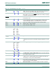
P0[6]/I2SRX_SDA/
LCDVD[8]/
SSEL1/MAT2[0]
164
[1]
D13
[1]
I/O P0[6] — General purpose digital input/output pin.
I/O I2SRX_SDA — I
2
S Receive data. It is driven by the transmitter and read
by the receiver. Corresponds to the signal SD in the I
2
S-bus
specification.
[15]
O LCDVD[8] — LCD data.
[15]
I/O SSEL1 — Slave Select for SSP1.
O MAT2[0] — Match output for Timer 2, channel 0.
P0[7]/I2STX_CLK/
LCDVD[9]/SCK1/
MAT2[1]
162
[1]
C13
[1]
I/O P0[7] — General purpose digital input/output pin.
I/O I2STX_CLK — I
2
S transmit clock. It is driven by the master and received
by the slave. Corresponds to the signal SCK in the I
2
S-bus
specification.
[15]
O LCDVD[9] — LCD data.
[15]
I/O SCK1 — Serial Clock for SSP1.
O MAT2[1] — Match output for Timer 2, channel 1.
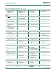
P0[8]/I2STX_WS/
LCDVD[16]/
MISO1/MAT2[2]
160
[1]
A15
[1]
I/O P0[8] — General purpose digital input/output pin.
I/O I2STX_WS — I
2
S Transmit word select. It is driven by the master and
received by the slave. Corresponds to the signal WS in the I
2
S-bus
specification.
[15]
O LCDVD[16] — LCD data.
[15]
I/O MISO1 — Master In Slave Out for SSP1.
O MAT2[2] — Match output for Timer 2, channel 2.
P0[9]/I2STX_SDA/
LCDVD[17]/
MOSI1/MAT2[3]
158
[1]
C14
[1]
I/O P0[9] — General purpose digital input/output pin.
I/O I2STX_SDA — I
2
S transmit data. It is driven by the transmitter and read
by the receiver. Corresponds to the signal SD in the I
2
S-bus
specification.
[15]
O LCDVD[17] — LCD data.
[15]
I/O MOSI1 — Master Out Slave In for SSP1.
O MAT2[3] — Match output for Timer 2, channel 3.
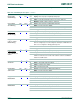
Table 124. LPC2470/78 pin description
…continued
Symbol Pin Ball Type Description