
Microcontrollers User manual


UM10237_2 © NXP B.V. 2008. All rights reserved.
User manual Rev. 02 — 19 December 2008 157 of 792
NXP Semiconductors
UM10237
Chapter 8: LPC24XX Pin configuration
9 P1[24]/USB_RX_DM1/
LCDVD[10]/LCDVD[14]/
PWM1[5]/MOSI0
10 P1[25]/USB_LS1/
LCDVD[11]/LCDVD[15]/
USB_HSTEN1
/MAT1[1]
11 P4[2]/A2 12 P1[27]/USB_INT1
/
LCDVD[13]/LCDVD[21]/
USB_OVRCR1
/CAP0[1]
13 P1[28]/USB_SCL1/
LCDVD[14]/LCDVD[22]/
PCAP1[0]/MAT0[0]
14 P0[1]/TD1/RXD3/SCL1 15 P0[10]/TXD2/SDA2/
MAT3[0]
16 P2[13]/EINT3
/
LCDVD[5]/LCDVD[9]/
LCDVD[19]/MCIDAT3/
I2STX_SDA
17 P2[11]/EINT1
/
LCDCLKIN/
MCIDAT1/I2STX_CLK
---
Row U
1 USB_D−22P3[25]/D25/
MAT0[0]/PWM1[2]
3 P2[18]/CLKOUT0 4 P0[29]/USB_D+1
5 P2[23]/DYCS3
/
CAP3[1]/SSEL0
6 P1[19]/USB_TX_E1/
USB_PPWR1/CAP1[1]
7 P1[20]/USB_TX_DP1/
LCDVD[6]/LCDVD[10]/
PWM1[2]/SCK0
8 P1[22]/USB_RCV1/
LCDVD[8]/LCDVD[12]/
USB_PWRD1/MAT1[0]
9 P4[0]/A0 10 P4[1]/A1 11 P2[21]/DYCS1
12 P2[22]/DYCS2/
CAP3[0]/SCK0
13 V
DD(3V3)
14 P1[29]/USB_SDA1/
LCDVD[15]/LCDVD[23]/
PCAP1[1]/MAT0[1]
15 P0[0]/RD1/TXD3/SDA1 16 P4[3]/A3
17 P4[16]/A16 - - -
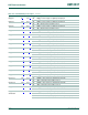
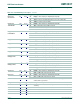
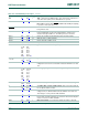
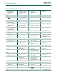
Table 123. LPC2470/78 pin allocation table
…continued
Pin Symbol Pin Symbol Pin Symbol Pin Symbol
Table 124. LPC2470/78 pin description
Symbol Pin Ball Type Description
P0[0] to P0[31] I/O Port 0: Port 0 is a 32-bit I/O port with individual direction controls for each
bit. The operation of port 0 pins depends upon the pin function selected
via the pin connect block.
P0[0]/RD1/TXD3/
SDA1
94
[1]
U15
[1]
I/O P0[0] — General purpose digital input/output pin.
I RD1 — CAN1 receiver input.
O TXD3 — Transmitter output for UART3.
I/O SDA1 — I
2
C1 data input/output (this is not an open-drain pin).
P0[1]/TD1/RXD3/
SCL1
96
[1]
T14
[1]
I/O P0[1] — General purpose digital input/output pin.
O TD1 — CAN1 transmitter output.
I RXD3 — Receiver input for UART3.
I/O SCL1 — I
2
C1 clock input/output (this is not an open-drain pin).
P0[2]/TXD0 202
[1]
C4
[1]
I/O P0[2] — General purpose digital input/output pin.
O TXD0 — Transmitter output for UART0.
P0[3]/RXD0 204
[1]
D6
[1]
I/O P0[3] — General purpose digital input/output pin.
I RXD0 — Receiver input for UART0.