
Microcontrollers User manual


UM10237_2 © NXP B.V. 2008. All rights reserved.
User manual Rev. 02 — 19 December 2008 147 of 792
NXP Semiconductors
UM10237
Chapter 8: LPC24XX Pin configuration
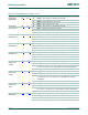
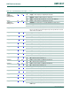
P2[15]/CS3/
CAP2[1]/SCL1
99
[6]
P13
[6]
I/O P2[15] — General purpose digital input/output pin.
O CS3
— LOW active Chip Select 3 signal.
I CAP2[1] — Capture input for Timer 2, channel 1.
I/O SCL1 — I
2
C1 clock input/output (this is not an open-drain pin).
P2[16]/CAS
87
[1]
R11
[1]
I/O P2[16] — General purpose digital input/output pin.
O CAS
— LOW active SDRAM Column Address Strobe.
P2[17]/RAS
95
[1]
R13
[1]
I/O P2[17] — General purpose digital input/output pin.
O RAS
— LOW active SDRAM Row Address Strobe.
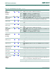
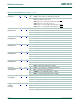
P2[18]/
CLKOUT0
59
[1]
U3
[1]
I/O P2[18] — General purpose digital input/output pin.
O CLKOUT0 — SDRAM clock 0.
P2[19]/
CLKOUT1
67
[1]
R7
[1]
I/O P2[19] — General purpose digital input/output pin.
O CLKOUT1 — SDRAM clock 1.
P2[20]/DYCS0
73
[1]
T8
[1]
I/O P2[20] — General purpose digital input/output pin.
O DYCS0
— SDRAM chip select 0.
P2[21]/DYCS1
81
[1]
U11
[1]
I/O P2[21] — General purpose digital input/output pin.
O DYCS1
— SDRAM chip select 1.
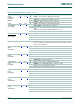
P2[22]/DYCS2
/
CAP3[0]/SCK0
85
[1]
U12
[1]
I/O P2[22] — General purpose digital input/output pin.
O DYCS2
— SDRAM chip select 2.
I CAP3[0] — Capture input for Timer 3, channel 0.
I/O SCK0 — Serial clock for SSP0.
P2[23]/DYCS3
/
CAP3[1]/SSEL0
64
[1]
U5
[1]
I/O P2[23] — General purpose digital input/output pin.
O DYCS3
— SDRAM chip select 3.
I CAP3[1] — Capture input for Timer 3, channel 1.
I/O SSEL0 — Slave Select for SSP0.
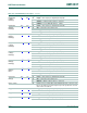
P2[24]/
CKEOUT0
53
[1]
P5
[1]
I/O P2[24] — General purpose digital input/output pin.
O CKEOUT0 — SDRAM clock enable 0.
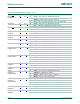
P2[25]/
CKEOUT1
54
[1]
R4
[1]
I/O P2[25] — General purpose digital input/output pin.
O CKEOUT1 — SDRAM clock enable 1.
P2[26]/
CKEOUT2/
MAT3[0]/MISO0
57
[1]
T4
[1]
I/O P2[26] — General purpose digital input/output pin.
O CKEOUT2 — SDRAM clock enable 2.
O MAT3[0] — Match output for Timer 3, channel 0.
I/O MISO0 — Master In Slave Out for SSP0.
P2[27]/
CKEOUT3/
MAT3[1]/MOSI0
47
[1]
P3
[1]
I/O P2[27] — General purpose digital input/output pin.
O CKEOUT3 — SDRAM clock enable 3.
O MAT3[1] — Match output for Timer 3, channel 1.
I/O MOSI0 — Master Out Slave In for SSP0.
P2[28]/
DQMOUT0
49
[1]
P4
[1]
I/O P2[28] — General purpose digital input/output pin.
O DQMOUT0 — Data mask 0 used with SDRAM and static devices.
P2[29]/
DQMOUT1
43
[1]
N3
[1]
I/O P2[29] — General purpose digital input/output pin.
O DQMOUT1 — Data mask 1 used with SDRAM and static devices.
Table 122. LPC2420/60/68 pin description
…continued
Symbol Pin Ball Type Description