
Microcontrollers User manual


UM10237_2 © NXP B.V. 2008. All rights reserved.
User manual Rev. 02 — 19 December 2008 146 of 792
NXP Semiconductors
UM10237
Chapter 8: LPC24XX Pin configuration
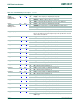
P2[6]/PCAP1[0]/
RI1/TRACEPKT1
138
[1]
E17
[1]
I/O P2[6] — General purpose digital input/output pin.
I PCAP1[0] — Capture input for PWM1, channel 0.
I RI1 — Ring Indicator input for UART1.
O TRACEPKT1 — Trace Packet, bit 1.
P2[7]/RD2/
RTS1/
TRACEPKT2
136
[1]
G16
[1]
I/O P2[7] — General purpose digital input/output pin.
I RD2 — CAN2 receiver input (LPC2460 only).
O RTS1 — Request to Send output for UART1.
O TRACEPKT2 — Trace Packet, bit 2.
P2[8]/TD2/
TXD2/
TRACEPKT3
134
[1]
H15
[1]
I/O P2[8] — General purpose digital input/output pin.
O TD2 — CAN2 transmitter output (LPC2460 only).
O TXD2 — Transmitter output for UART2.
O TRACEPKT3 — Trace Packet, bit 3.
P2[9]/
USB_CONNECT1/
RXD2/
EXTIN0
132
[1]
H16
[1]
I/O P2[9] — General purpose digital input/output pin.
O USB_CONNECT1 — USB1 SoftConnect control. Signal used to switch
an external 1.5 kΩ resistor under the software control. Used with the
SoftConnect USB feature.
I RXD2 — Receiver input for UART2.
I EXTIN0 — External Trigger Input.
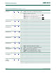
P2[10]/EINT0
110
[6]
N15
[6]
I/O P2[10] — General purpose digital input/output pin.
Note: LOW on this pin while RESET is LOW forces on-chip bootloader to
take over control of the part after a reset.
I EINT0 — External interrupt 0 input.
P2[11]/EINT1
/
MCIDAT1/
I2STX_CLK
108
[6]
T17
[6]
I/O P2[11] — General purpose digital input/output pin.
I EINT1
— External interrupt 1 input.
I/O MCIDAT1 — Data line 1 for SD/MMC interface.
I/O I2STX_CLK — Transmit Clock. It is driven by the master and received by
the slave. Corresponds to the signal SCK in the I
2
S-bus specification.
P2[12]/EINT2
/
MCIDAT2/
I2STX_WS
106
[6]
N14
[6]
I/O P2[12] — General purpose digital input/output pin.
I EINT2
— External interrupt 2 input.
I/O MCIDAT2 — Data line 2 for SD/MMC interface.
I/O I2STX_WS — Transmit Word Select. It is driven by the master and
received by the slave. Corresponds to the signal WS in the I
2
S-bus
specification.
P2[13]/EINT3
/
MCIDAT3/
I2STX_SDA
102
[6]
T16
[6]
I/O P2[13] — General purpose digital input/output pin.
I EINT3
— External interrupt 3 input.
I/O MCIDAT3 — Data line 3 for SD/MMC interface.
I/O I2STX_SDA — Transmit data. It is driven by the transmitter and read by
the receiver. Corresponds to the signal SD in the I
2
S-bus specification.
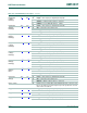
P2[14]/CS2
/
CAP2[0]/SDA1
91
[6]
R12
[6]
I/O P2[14] — General purpose digital input/output pin.
O CS2
— LOW active Chip Select 2 signal.
I CAP2[0] — Capture input for Timer 2, channel 0.
I/O SDA1 — I
2
C1 data input/output (this is not an open-drain pin).
Table 122. LPC2420/60/68 pin description
…continued
Symbol Pin Ball Type Description