
Microcontrollers User manual


UM10237_2 © NXP B.V. 2008. All rights reserved.
User manual Rev. 02 — 19 December 2008 144 of 792
NXP Semiconductors
UM10237
Chapter 8: LPC24XX Pin configuration
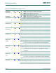
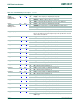
P1[19]/
USB_TX_E1/
USB_PPWR1
/
CAP1[1]
68
[1]
U6
[1]
I/O P1[19] — General purpose digital input/output pin.
O USB_TX_E1
— Transmit Enable signal for USB port 1 (OTG transceiver).
O USB_PPWR1
— Port Power enable signal for USB port 1.
I CAP1[1] — Capture input for Timer 1, channel 1.
P1[20]/
USB_TX_DP1/
PWM1[2]/SCK0
70
[1]
U7
[1]
I/O P1[20] — General purpose digital input/output pin.
O USB_TX_DP1 — D+ transmit data for USB port 1 (OTG transceiver).
O PWM1[2] — Pulse Width Modulator 1, channel 2 output.
I/O SCK0 — Serial clock for SSP0.
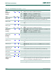
P1[21]/
USB_TX_DM1/
PWM1[3]/SSEL0
72
[1]
R8
[1]
I/O P1[21] — General purpose digital input/output pin.
O USB_TX_DM1 — D− transmit data for USB port 1 (OTG transceiver).
O PWM1[3] — Pulse Width Modulator 1, channel 3 output.
I/O SSEL0 — Slave Select for SSP0.
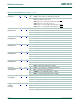
P1[22]/
USB_RCV1/
USB_PWRD1/
MAT1[0]
74
[1]
U8
[1]
I/O P1[22] — General purpose digital input/output pin.
I USB_RCV1 — Differential receive data for USB port 1 (OTG transceiver).
I USB_PWRD1 — Power Status for USB port 1 (host power switch).
O MAT1[0] — Match output for Timer 1, channel 0.
P1[23]/
USB_RX_DP1/
PWM1[4]/MISO0
76
[1]
P9
[1]
I/O P1[23] — General purpose digital input/output pin.
I USB_RX_DP1 — D+ receive data for USB port 1 (OTG transceiver).
O PWM1[4] — Pulse Width Modulator 1, channel 4 output.
I/O MISO0 — Master In Slave Out for SSP0.
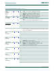
P1[24]/
USB_RX_DM1/
PWM1[5]/MOSI0
78
[1]
T9
[1]
I/O P1[24] — General purpose digital input/output pin.
I USB_RX_DM1 — D− receive data for USB port 1 (OTG transceiver).
O PWM1[5] — Pulse Width Modulator 1, channel 5 output.
I/O MOSI0 — Master Out Slave in for SSP0.
P1[25]/
USB_LS1
/
USB_HSTEN1
/
MAT1[1]
80
[1]
T10
[1]
I/O P1[25] — General purpose digital input/output pin.
O USB_LS1
— Low-speed status for USB port 1 (OTG transceiver).
O USB_HSTEN1
— Host Enabled status for USB port 1.
O MAT1[1] — Match output for Timer 1, channel 1.
P1[26]/
USB_SSPND1
/
PWM1[6]/
CAP0[0]
82
[1]
R10
[1]
I/O P1[26] — General purpose digital input/output pin.
O USB_SSPND1
— USB port 1 Bus Suspend status (OTG transceiver).
O PWM1[6] — Pulse Width Modulator 1, channel 6 output.
I CAP0[0] — Capture input for Timer 0, channel 0.
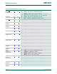
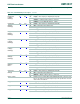
P1[27]/
USB_INT1
/
USB_OVRCR1
/
CAP0[1]
88
[1]
T12
[1]
I/O P1[27] — General purpose digital input/output pin.
I USB_INT1
— USB port 1 OTG transceiver interrupt (OTG transceiver).
I USB_OVRCR1
— USB port 1 Over-Current status.
I CAP0[1] — Capture input for Timer 0, channel 1.
P1[28]/
USB_SCL1/
PCAP1[0]/
MAT0[0]
90
[1]
T13
[1]
I/O P1[28] — General purpose digital input/output pin.
I/O USB_SCL1 — USB port 1 I
2
C serial clock (OTG transceiver).
I PCAP1[0] — Capture input for PWM1, channel 0.
O MAT0[0] — Match output for Timer 0, channel 0.
Table 122. LPC2420/60/68 pin description
…continued
Symbol Pin Ball Type Description