
Microcontrollers User manual


UM10237_2 © NXP B.V. 2008. All rights reserved.
User manual Rev. 02 — 19 December 2008 139 of 792
NXP Semiconductors
UM10237
Chapter 8: LPC24XX Pin configuration
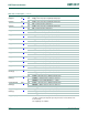
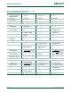
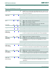
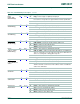
Table 122. LPC2420/60/68 pin description
Symbol Pin Ball Type Description
P0[0] to P0[31] I/O Port 0: Port 0 is a 32-bit I/O port with individual direction controls for each
bit. The operation of port 0 pins depends upon the pin function selected
via the Pin Connect block.
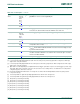
P0[0]/RD1/
TXD3/SDA1
94
[1]
U15
[1]
I/O P0[0] — General purpose digital input/output pin.
I RD1 — CAN1 receiver input (LPC2460 only).
O TXD3 — Transmitter output for UART3.
I/O SDA1 — I
2
C1 data input/output (this is not an open-drain pin).
P0[1]/TD1/RXD3/
SCL1
96
[1]
T14
[1]
I/O P0[1] — General purpose digital input/output pin.
O TD1 — CAN1 transmitter output (LPC2460 only).
I RXD3 — Receiver input for UART3.
I/O SCL1 — I
2
C1 clock input/output (this is not an open-drain pin).
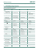
P0[2]/TXD0 202
[1]
C4
[1]
I/O P0[2] — General purpose digital input/output pin.
O TXD0 — Transmitter output for UART0.
P0[3]/RXD0 204
[1]
D6
[1]
I/O P0[3] — General purpose digital input/output pin.
I RXD0 — Receiver input for UART0.
P0[4]/
I2SRX_CLK/
RD2/CAP2[0]
168
[1]
B12
[1]
I/O P0[4] — General purpose digital input/output pin.
I/O I2SRX_CLK — Receive Clock. It is driven by the master and received by
the slave. Corresponds to the signal SCK in the I
2
S-bus specification.
I RD2 — CAN2 receiver input (LPC2460 only).
I CAP2[0] — Capture input for Timer 2, channel 0.
P0[5]/
I2SRX_WS/
TD2/CAP2[1]
166
[1]
C12
[1]
I/O P0[5] — General purpose digital input/output pin.
I/O I2SRX_WS — Receive Word Select. It is driven by the master and
received by the slave. Corresponds to the signal WS in the I
2
S-bus
specification.
O TD2 — CAN2 transmitter output (LPC2460 only).
I CAP2[1] — Capture input for Timer 2, channel 1.
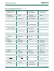
P0[6]/
I2SRX_SDA/
SSEL1/MAT2[0]
164
[1]
D13
[1]
I/O P0[6] — General purpose digital input/output pin.
I/O I2SRX_SDA — Receive data. It is driven by the transmitter and read by
the receiver. Corresponds to the signal SD in the I
2
S-bus specification.
I/O SSEL1 — Slave Select for SSP1.
O MAT2[0] — Match output for Timer 2, channel 0.
P0[7]/
I2STX_CLK/
SCK1/MAT2[1]
162
[1]
C13
[1]
I/O P0[7] — General purpose digital input/output pin.
I/O I2STX_CLK — Transmit Clock. It is driven by the master and received by
the slave. Corresponds to the signal SCK in the I
2
S-bus specification.
I/O SCK1 — Serial Clock for SSP1.
O MAT2[1] — Match output for Timer 2, channel 1.
P0[8]/
I2STX_WS/
MISO1/MAT2[2]
160
[1]
A15
[1]
I/O P0[8] — General purpose digital input/output pin.
I/O I2STX_WS — Transmit Word Select. It is driven by the master and
received by the slave. Corresponds to the signal WS in the I
2
S-bus
specification.
I/O MISO1 — Master In Slave Out for SSP1.
O MAT2[2] — Match output for Timer 2, channel 2.