
Microcontrollers User manual


UM10237_2 © NXP B.V. 2008. All rights reserved.
User manual Rev. 02 — 19 December 2008 134 of 792
NXP Semiconductors
UM10237
Chapter 8: LPC24XX Pin configuration
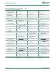
P4[24]/OE C8
[1]
I/O P4[24] — General purpose digital input/output pin.
O OE
— LOW active Output Enable signal.
P4[25]/WE
D9
[1]
I/O P4[25] — General purpose digital input/output pin.
O WE
— LOW active Write Enable signal.
P4[26]/BLS0 K13
[1]
I/O P4[26] — General purpose digital input/output pin.
O BLS0 — LOW active Byte Lane select signal 0.
P4[27]/BLS1 F14
[1]
I/O P4[27] — General purpose digital input/output pin.
O BLS1 — LOW active Byte Lane select signal 1.
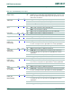
P4[28]/MAT2[0]/
TXD3
D10
[1]
I/O P4[28] — General purpose digital input/output pin.
O MAT2[0] — Match output for Timer 2, channel 0.
O TXD3 — Transmitter output for UART3.
P4[29]/MAT2[1]/
RXD3
B9
[1]
I/O P4[29] — General purpose digital input/output pin.
O MAT2[1] — Match output for Timer 2, channel 1.
I RXD3 — Receiver input for UART3.
P4[30]/CS0
C7
[1]
I/O P4[30] — General purpose digital input/output pin.
O CS0
— LOW active Chip Select 0 signal.
P4[31]/CS1
E7
[1]
I/O P4[31] — General purpose digital input/output pin.
O CS1
— LOW active Chip Select 1 signal.
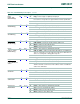
ALARM H5
[8]
O ALARM — RTC controlled output. This is a 1.8 V pin. It goes HIGH when a RTC
alarm is generated.
USB_D−2N2I/OUSB_D−2 — USB port 2 bidirectional D− line.
DBGEN E5
[1]
I DBGEN — JTAG interface control signal. Also used for boundary scan.
TDO B1
[1]
O TDO — Test Data Out for JTAG interface.
TDI C3
[1]
I TDI — Test Data In for JTAG interface.
TMS C2
[1]
I TMS — Test Mode Select for JTAG interface.
TRST
D4
[1]
I TRST — Test Reset for JTAG interface.
TCK D2
[1]
I TCK — Test Clock for JTAG interface. This clock must be slower than
1
⁄
6
of the
CPU clock (CCLK) for the JTAG interface to operate.
RTCK C4
[1]
I/O RTCK — JTAG interface control signal.
Note: LOW on this pin while RESET
is LOW enables ETM pins (P2[9:0]) to
operate as Trace port after reset.
RSTOUT
H2 O RSTOUT — This is a 3.3 V pin. LOW on this pin indicates UM10237 being in
Reset state.
RESET
J1
[7]
I external reset input: A LOW on this pin resets the device, causing I/O ports and
peripherals to take on their default states, and processor execution to begin at
address 0. TTL with hysteresis, 5 V tolerant.
XTAL1 L2
[8]
I Input to the oscillator circuit and internal clock generator circuits.
XTAL2 K4
[8]
O Output from the oscillator amplifier.
RTCX1 J2
[8]
I Input to the RTC oscillator circuit.
RTCX2 J3
[8]
O Output from the RTC oscillator circuit.
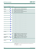
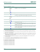
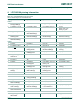
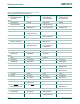
Table 120. Pin description
…continued
Symbol Ball Type Description