
Microcontrollers User manual


UM10237_2 © NXP B.V. 2008. All rights reserved.
User manual Rev. 02 — 19 December 2008 131 of 792
NXP Semiconductors
UM10237
Chapter 8: LPC24XX Pin configuration
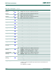
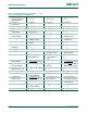
P2[12]/EINT2/
MCIDAT2/
I2STX_WS
N14
[6]
I/O P2[12] — General purpose digital input/output pin.
I EINT2
— External interrupt 2 input.
I/O MCIDAT2 — Data line 2 for SD/MMC interface.
I/O I2STX_WS — Transmit Word Select. It is driven by the master and received by
the slave. Corresponds to the signal WS in the I
2
S-bus specification.
P2[13]/EINT3
/
MCIDAT3/
I2STX_SDA
M11
[6]
I/O P2[13] — General purpose digital input/output pin.
I EINT3
— External interrupt 3 input.
I/O MCIDAT3 — Data line 3 for SD/MMC interface.
I/O I2STX_SDA — Transmit data. It is driven by the transmitter and read by the
receiver. Corresponds to the signal SD in the I
2
S-bus specification.
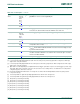
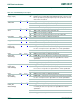
P2[16]/CAS
P9
[1]
I/O P2[16] — General purpose digital input/output pin.
O CAS
— LOW active SDRAM Column Address Strobe.
P2[17]/RAS
P11
[1]
I/O P2[17] — General purpose digital input/output pin.
O RAS
— LOW active SDRAM Row Address Strobe.
P2[18]/
CLKOUT0
P3
[1]
I/O P2[18] — General purpose digital input/output pin.
O CLKOUT0 — SDRAM clock 0.
P2[19]/
CLKOUT1
N5
[1]
I/O P2[19] — General purpose digital input/output pin.
O CLKOUT1 — SDRAM clock 1.
P2[20]/DYCS0
P6
[1]
I/O P2[20] — General purpose digital input/output pin.
O DYCS0
— SDRAM chip select 0.
P2[21]/DYCS1
N8
[1]
I/O P2[21] — General purpose digital input/output pin.
O DYCS1
— SDRAM chip select 1.
P2[24]/
CKEOUT0
P1
[1]
I/O P2[24] — General purpose digital input/output pin.
O CKEOUT0 — SDRAM clock enable 0.
P2[25]/
CKEOUT1
P2
[1]
I/O P2[25] — General purpose digital input/output pin.
O CKEOUT1 — SDRAM clock enable 1.
P2[28]/
DQMOUT0
M2
[1]
I/O P2[28] — General purpose digital input/output pin.
O DQMOUT0 — Data mask 0 used with SDRAM and static devices.
P2[29]/
DQMOUT1
L1
[1]
I/O P2[29] — General purpose digital input/output pin.
O DQMOUT1 — Data mask 1 used with SDRAM and static devices.
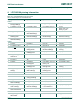
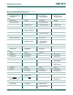
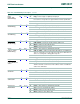
P3[0] to P3[31] I/O Port 3: Port 3 is a 32-bit I/O port with individual direction controls for each bit. The
operation of port 3 pins depends upon the pin function selected via the Pin
Connect block.
Pins P3[16:22] and P3[27:31] are not available.
P3[0]/D0 D6
[1]
I/O P3[0] — General purpose digital input/output pin.
I/O D0 — External memory data line 0.
P3[1]/D1 E6
[1]
I/O P3[1] — General purpose digital input/output pin.
I/O D1 — External memory data line 1.
P3[2]/D2 A2
[1]
I/O P3[2] — General purpose digital input/output pin.
I/O D2 — External memory data line 2.
P3[3]/D3 G5
[1]
I/O P3[3] — General purpose digital input/output pin.
I/O D3 — External memory data line 3.
Table 120. Pin description
…continued
Symbol Ball Type Description