
Microcontrollers User manual


UM10237_2 © NXP B.V. 2008. All rights reserved.
User manual Rev. 02 — 19 December 2008 129 of 792
NXP Semiconductors
UM10237
Chapter 8: LPC24XX Pin configuration
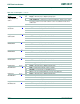
P1[26]/
USB_SSPND1/
PWM1[6]/
CAP0[0]
P8
[1]
I/O P1[26] — General purpose digital input/output pin.
O USB_SSPND1
— USB port 1 Bus Suspend status (OTG transceiver).
O PWM1[6] — Pulse Width Modulator 1, channel 6 output.
I CAP0[0] — Capture input for Timer 0, channel 0.
P1[27]/
USB_INT1
/
USB_OVRCR1
/
CAP0[1]
M9
[1]
I/O P1[27] — General purpose digital input/output pin.
I USB_INT1
— USB port 1 OTG transceiver interrupt.
I USB_OVRCR1
— USB port 1 Over-Current status.
I CAP0[1] — Capture input for Timer 0, channel 1.
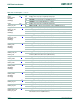
P1[28]/
USB_SCL1/
PCAP1[0]/
MAT0[0]
P10
[1]
I/O P1[28] — General purpose digital input/output pin.
I/O USB_SCL1 — USB port 1 I
2
C serial clock (OTG transceiver).
I PCAP1[0] — Capture input for PWM1, channel 0.
O MAT0[0] — Match output for Timer 0, channel 0.
P1[29]/
USB_SDA1/
PCAP1[1]/
MAT0[1]
N10
[1]
I/O P1[29] — General purpose digital input/output pin.
I/O USB_SDA1 — USB port 1 I
2
C serial data (OTG transceiver).
I PCAP1[1] — Capture input for PWM1, channel 1.
O MAT0[1] — Match output for Timer 0, channel 0.
P1[30]/
USB_PWRD2/
V
BUS
/AD0[4]
K3
[2]
I/O P1[30] — General purpose digital input/output pin.
I USB_PWRD2 — Power Status for USB port 2.
I V
BUS
— Monitors the presence of USB bus power.
Note: This signal must be HIGH for USB reset to occur.
I AD0[4] — A/D converter 0, input 4.
P1[31]/
USB_OVRCR2
/
SCK1/AD0[5]
K2
[2]
I/O P1[31] — General purpose digital input/output pin.
I USB_OVRCR2
— Over-Current status for USB port 2.
I/O SCK1 — Serial Clock for SSP1.
I AD0[5] — A/D converter 0, input 5.
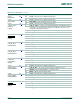
P2[0] to P2[31] I/O Port 2: Port 2 is a 32-bit I/O port with individual direction controls for each bit. The
operation of port 2 pins depends upon the pin function selected via the Pin
Connect block.
Pins P2[14:15], P2[22:23], P2[26:27] and P2[30:31] are not available.
P2[0]/PWM1[1]/
TXD1/
TRACECLK
D12
[1]
I/O P2[0] — General purpose digital input/output pin.
O PWM1[1] — Pulse Width Modulator 1, channel 1 output.
O TXD1 — Transmitter output for UART1.
O TRACECLK — Trace Clock.
P2[1]/PWM1[2]/
RXD1/
PIPESTAT0
C14
[1]
I/O P2[1] — General purpose digital input/output pin.
O PWM1[2] — Pulse Width Modulator 1, channel 2 output.
I RXD1 — Receiver input for UART1.
O PIPESTAT0 — Pipeline Status, bit 0.
P2[2]/PWM1[3]/
CTS1/
PIPESTAT1
E11
[1]
I/O P2[2] — General purpose digital input/output pin.
O PWM1[3] — Pulse Width Modulator 1, channel 3 output.
I CTS1 — Clear to Send input for UART1.
O PIPESTAT1 — Pipeline Status, bit 1.
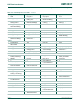
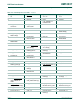
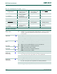
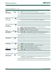
Table 120. Pin description
…continued
Symbol Ball Type Description