
Microcontrollers User manual


UM10237_2 © NXP B.V. 2008. All rights reserved.
User manual Rev. 02 — 19 December 2008 125 of 792
NXP Semiconductors
UM10237
Chapter 8: LPC24XX Pin configuration
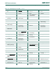
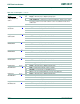
P0[14]/
USB_HSTEN2/
USB_CONNECT2/
SSEL1
M5
[1]
I/O P0[14] — General purpose digital input/output pin.
O USB_HSTEN2
— Host Enabled status for USB port 2.
O USB_CONNECT2 — SoftConnect control for USB port 2. Signal used to switch
an external 1.5 kΩ resistor under software control. Used with the SoftConnect
USB feature.
I/O SSEL1 — Slave Select for SSP1.
P0[15]/TXD1/
SCK0/SCK
H13
[1]
I/O P0[15] — General purpose digital input/output pin.
O TXD1 — Transmitter output for UART1.
I/O SCK0 — Serial clock for SSP0.
I/O SCK — Serial clock for SPI.
P0[16]/RXD1/
SSEL0/SSEL
H14
[1]
I/O P0[16] — General purpose digital input/output pin.
I RXD1 — Receiver input for UART1.
I/O SSEL0 — Slave Select for SSP0.
I/O SSEL — Slave Select for SPI.
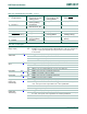
P0[17]/CTS1/
MISO0/MISO
J12
[1]
I/O P0[17] — General purpose digital input/output pin.
I CTS1 — Clear to Send input for UART1.
I/O MISO0 — Master In Slave Out for SSP0.
I/O MISO — Master In Slave Out for SPI.
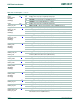
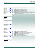
P0[18]/DCD1/
MOSI0/MOSI
J13
[1]
I/O P0[18] — General purpose digital input/output pin.
I DCD1 — Data Carrier Detect input for UART1.
I/O MOSI0 — Master Out Slave In for SSP0.
I/O MOSI — Master Out Slave In for SPI.
P0[19]/DSR1/
MCICLK/SDA1
J10
[1]
I/O P0[19] — General purpose digital input/output pin.
I DSR1 — Data Set Ready input for UART1.
O MCICLK — Clock output line for SD/MMC interface.
I/O SDA1 — I
2
C1 data input/output (this is not an open-drain pin).
P0[20]/DTR1/
MCICMD/SCL1
K14
[1]
I/O P0[20] — General purpose digital input/output pin.
O DTR1 — Data Terminal Ready output for UART1.
I/O MCICMD — Command line for SD/MMC interface.
I/O SCL1 — I
2
C1 clock input/output (this is not an open-drain pin).
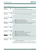
P0[21]/RI1/
MCIPWR/RD1
K11
[1]
I/O P0[21] — General purpose digital input/output pin.
I RI1 — Ring Indicator input for UART1.
O MCIPWR — Power Supply Enable for external SD/MMC power supply.
I RD1 — CAN1 receiver input.
P0[22]/RTS1/
MCIDAT0/TD1
L14
[1]
I/O P0[22] — General purpose digital input/output pin.
O RTS1 — Request to Send output for UART1.
I/O MCIDAT0 — Data line 0 for SD/MMC interface.
O TD1 — CAN1 transmitter output.
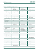
Table 120. Pin description
…continued
Symbol Ball Type Description