
Microcontrollers User manual


UM10237_2 © NXP B.V. 2008. All rights reserved.
User manual Rev. 02 — 19 December 2008 124 of 792
NXP Semiconductors
UM10237
Chapter 8: LPC24XX Pin configuration
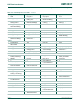
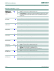
P0[6]/
I2SRX_SDA/
SSEL1/MAT2[0]
D11
[1]
I/O P0[6] — General purpose digital input/output pin.
I/O I2SRX_SDA — Receive data. It is driven by the transmitter and read by the
receiver. Corresponds to the signal SD in the I
2
S-bus specification.
I/O SSEL1 — Slave Select for SSP1.
O MAT2[0] — Match output for Timer 2, channel 0.
P0[7]/
I2STX_CLK/
SCK1/MAT2[1]
B12
[1]
I/O P0[7] — General purpose digital input/output pin.
I/O I2STX_CLK — Transmit Clock. It is driven by the master and received by the
slave. Corresponds to the signal SCK in the I
2
S-bus specification.
I/O SCK1 — Serial Clock for SSP1.
O MAT2[1] — Match output for Timer 2, channel 1.
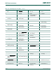
P0[8]/
I2STX_WS/
MISO1/MAT2[2]
C12
[1]
I/O P0[8] — General purpose digital input/output pin.
I/O I2STX_WS — Transmit Word Select. It is driven by the master and received by
the slave. Corresponds to the signal WS in the I
2
S-bus specification.
I/O MISO1 — Master In Slave Out for SSP1.
O MAT2[2] — Match output for Timer 2, channel 2.
P0[9]/
I2STX_SDA/
MOSI1/MAT2[3]
A13
[1]
I/O P0[9] — General purpose digital input/output pin.
I/O I2STX_SDA — Transmit data. It is driven by the transmitter and read by the
receiver. Corresponds to the signal SD in the I
2
S-bus specification.
I/O MOSI1 — Master Out Slave In for SSP1.
O MAT2[3] — Match output for Timer 2, channel 3.
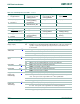
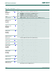
P0[10]/TXD2/
SDA2/MAT3[0]
L10
[1]
I/O P0[10] — General purpose digital input/output pin.
O TXD2 — Transmitter output for UART2.
I/O SDA2 — I
2
C2 data input/output (this is not an open-drain pin).
O MAT3[0] — Match output for Timer 3, channel 0.
P0[11]/RXD2/
SCL2/MAT3[1]
P12
[1]
I/O P0[11] — General purpose digital input/output pin.
I RXD2 — Receiver input for UART2.
I/O SCL2 — I
2
C2 clock input/output (this is not an open-drain pin).
O MAT3[1] — Match output for Timer 3, channel 1.
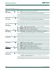
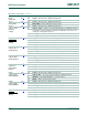
P0[12]/
USB_PPWR2
/
MISO1/AD0[6]
J4
[2]
I/O P0[12] — General purpose digital input/output pin.
O USB_PPWR2
— Port Power enable signal for USB port 2.
I/O MISO1 — Master In Slave Out for SSP1.
I AD0[6] — A/D converter 0, input 6.
P0[13]/
USB_UP_LED2/
MOSI1/AD0[7]
J5
[2]
I/O P0[13] — General purpose digital input/output pin.
O USB_UP_LED2 — USB port 2 GoodLink LED indicator. It is LOW when device is
configured (non-control endpoints enabled). It is HIGH when the device is not
configured or during global suspend.
I/O MOSI1 — Master Out Slave In for SSP1.
I AD0[7] — A/D converter 0, input 7.
Table 120. Pin description
…continued
Symbol Ball Type Description