
Datasheet


LPC1850_30_20_10 All information provided in this document is subject to legal disclaimers. © NXP Semiconductors N.V. 2014. All rights reserved.
Product data sheet Rev. 6.4 — 18 August 2014 144 of 150
NXP Semiconductors
LPC1850/30/20/10
32-bit ARM Cortex-M3 microcontroller
18. Revision history
Table 40. Revision history
Document ID Release date Data sheet status Change notice Supersedes
LPC1850_30_20_10 v.6.4 20140818 Product data sheet - LPC1850_30_20_10 v.6.3
Modifications:
• IEEE standard 802.3 compliance added to Section 11.13. Covers Ethernet dynamic
characteristics of ENET_MDIO and ENET_MDC signals.
• Parameter C
I
corrected for high-drive pins (changed from 2 pF to 5.2 pF). See
Table 10.
• Table 18 “Dynamic characteristic: I/O pins
[1]
” added.
• IRC accuracy changed from 1 % to 1.5 % over the full temperature range. See Table
16 “Dynamic characteristic: IRC oscillator”.
• Description of internal pull-up resistor configuration added for RESET, WAKEUPn,
and ALARM pins. See Table 3
.
• Description of DEBUG pin updated.
• Input range for PLL1 corrected: 1 MHz to 25 MHz. See Section 7.18.7 “System PLL1”.
• Section 13.7 “Suggested USB interface solutions” added.
• Reset state of the RTC alarm pin RTC_ALARM added. See Table 3.
• Signal polarity corrected for signals EMC_CKEOUT and EMC_DQMOUT. Both
signals are active HIGH.
• SPIFI output timing parameters in Tabl e 31 corrected to apply to Mode 0:
– t
v(Q)
changed to 3.2 ns.
– t
h(Q)
changed to 0.2 ns,
• Parameter t
CSLWEL
with condition PB = 1 corrected: (WAITWEN + 1) T
cy(clk)
added.
See Table 23 “
Dynamic characteristics: Static asynchronous external memory
interface”.
• Parameter t
CSLBLSL
with condition PB = 0 corrected: (WAITWEN + 1) T
cy(clk)
added.
See Table 23 “
Dynamic characteristics: Static asynchronous external memory
interface”.
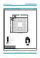
• SSP master mode timing diagram updated with SSEL timing parameters. See Figure
29 “SSP master timing in SPI mode”.
• Parameters t
lead
, t
lag
, and t
d
added in Table 22 “Dynamic characteristics: SSP pins in
SPI mode”.
LPC1850_30_20_10 v.6.3 20131210 Product data sheet - LPC1850_30_20_10 v.6.2
Modifications:
• Maximum value for V
i(RMS)
added in Section 13.3 “RTC oscillator”.
• V
O
for RTC_ALARM pin added in Table 10.
• RTC_ALARM and WAKEUPn pins added to Table 10.