
- Philips Semiconductors Logic level TOPFET Specification Sheet
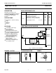

Philips Semiconductors Product specification
Logic level TOPFET PIP3119-P
LIMITING VALUES
Limiting values in accordance with the Absolute Maximum Rating System (IEC 134)
SYMBOL PARAMETER CONDITIONS MIN. MAX. UNIT
V
DS
Continuous drain source voltage
1
-50V
I
D
Continuous drain current V
IS
= 5 V; T
mb
=
25˚C - self - A
limited
I
D
Continuous drain current V
IS
= 5 V; T
mb
≤
121˚C - 20 A
I
I
Continuous input current -5 5 mA
I
IRM
Repetitive peak input current δ ≤ 0.1, tp = 300 µs -50 50 mA
P
D
Total power dissipation T
mb
≤ 25˚C - 90 W
T
stg
Storage temperature -55 175 ˚C
T
j
Continuous junction temperature
2
normal operation - 150 ˚C
T
sold
Lead temperature during soldering - 260 ˚C
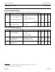
ESD LIMITING VALUE
SYMBOL PARAMETER CONDITIONS MIN. MAX. UNIT
V
C
Electrostatic discharge capacitor Human body model; - 2 kV
voltage C = 250 pF; R = 1.5 kΩ
OVERVOLTAGE CLAMPING LIMITING VALUES
At a drain source voltage above 50 V the power MOSFET is actively turned on to clamp overvoltage transients.
SYMBOL PARAMETER CONDITIONS MIN. MAX. UNIT
Inductive load turn-off I
DM
= 20 A; V
DD
≤ 20 V
E
DSM
Non-repetitive clamping energy T
mb
≤ 25˚C - 350 mJ
E
DRM
Repetitive clamping energy T
mb
≤ 95˚C; f = 250 Hz - 45 mJ
OVERLOAD PROTECTION LIMITING VALUE
With an adequate protection supply provided via the input pin, TOPFET can protect itself from two types of overload
- overtemperature and short circuit load.
SYMBOL PARAMETER REQUIRED CONDITION MIN. MAX. UNIT
V
DS
Drain source voltage
3
4 V ≤ V
IS
≤ 5.5 V 0 35 V
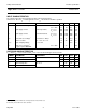
THERMAL CHARACTERISTIC
SYMBOL PARAMETER CONDITIONS MIN. TYP. MAX. UNIT
Thermal resistance
R
th j-mb
Junction to mounting base - - 1.25 1.39 K/W
1 Prior to the onset of overvoltage clamping. For voltages above this value, safe operation is limited by the overvoltage clamping energy.
2 A higher T
j
is allowed as an overload condition but at the threshold T
j(TO)
the over temperature trip operates to protect the switch.
3 All control logic and protection functions are disabled during conduction of the source drain diode.
May 2001 2 Rev 1.000