
Datasheet

CBTW28DD14 All information provided in this document is subject to legal disclaimers. © NXP Semiconductors N.V. 2014. All rights reserved.
Product data sheet Rev. 6 — 25 July 2014 4 of 13
NXP Semiconductors
CBTW28DD14
14-bit bus switch/multiplexer for DDR2/DDR3/DDR4 applications
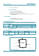
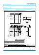
7. Functional description
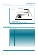
Refer to Figure 1 “Functional diagram”.
The CBTW28DD14 uses a 1.5 V or 1.8 V power supply. All signal paths are implemented
using high-bandwidth pass-gate technology and are non-directional. No clock or reset
signal is needed for the multiplexer to function. The switch position for the channels is
selected using the select signal SEL. The detailed operation is described in Section 7.1
.
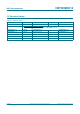
7.1 Function selection
The internal multiplexer switch position is controlled by two logic inputs, SEL and EN, as
described in Table 4
.
When a channel is not being used, Port B and Port C of this channel should be tied to
ground. For example, if Channel 2 is not used, B2 and C2 should be tied to ground and A2
should be left open.
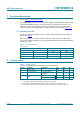
8. Limiting values
[1] Human Body Model: ANSI/EOS/ESD-S5.1-1994, standard for ESD sensitivity testing. Human Body Model -
Component level; Electrostatic Discharge Association, Rome, NY, USA.
[2] Charged-Device Model: ANSI/EOS/ESD-S5.3-1-1999, standard for ESD sensitivity testing,
Charged-Device Model - Component level; Electrostatic Discharge Association, Rome, NY, USA.
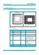
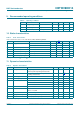
Table 4. Function selection
X = don’t care.
Inputs Switch position
EN SEL A B A C
LOW X OFF (isolating) OFF (isolating)
HIGH LOW ON (conducting) OFF (isolating)
HIGH HIGH OFF (isolating) ON (conducting)
Table 5. Limiting values
In accordance with the Absolute Maximum Rating System (IEC 60134).
Symbol Parameter Conditions Min Max Unit
V
DD
supply voltage 0.3 +2.5 V
T
case
case temperature for operation within
specification
40 +85 C
V
ESD
electrostatic discharge
voltage
HBM
[1]
- 3000 V
CDM
[2]
- 1000 V