
Datasheet

CBTW28DD14 All information provided in this document is subject to legal disclaimers. © NXP Semiconductors N.V. 2014. All rights reserved.
Product data sheet Rev. 6 — 25 July 2014 3 of 13
NXP Semiconductors
CBTW28DD14
14-bit bus switch/multiplexer for DDR2/DDR3/DDR4 applications
6. Pinning information
6.1 Pinning
6.2 Pin description
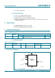
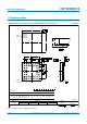
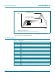
Fig 2. Pin configuration for TFBGA48 Fig 3. Ball mapping
002aae970
CBTW28DD14ET
Transparent top view
H
G
F
D
B
E
C
A
24681357
ball A1
index area
B9
1
A
B10B
B11C
C11D
B12E
B13F
A13G
A12H
B8
2
C9
C10
EN
C12
C13
A11
A10
B7
3
C8
A9
A8
C7
4
GND
GND
A7
C6
5
V
DD
V
DD
A6
B6
6
C5
A4
A5
B5
7
C4
C3
SEL
C1
C0
A2
A3
B4
8
B3
B2
C2
B1
B0
A0
A1
002aae971
Transparent top view
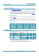
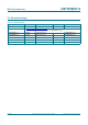
Table 3. Pin description
Symbol Pin Type Description
A[0:13] G8, H8, G7, H7, G6, H6, H5,
H4, H3, G3, H2, G2, H1, G1
high-speed I/O 14-bit wide input/output, port A
B[0:13] F8, E8, C8, B8, A8, A7, A6,
A3, A2, A1, B1, C1, E1, F1
high-speed I/O 14-bit wide input/output, port B
C[0:13] F7, E7, D8, C7, B7, B6, A5,
A4, B3, B2, C2, D1, E2, F2
high-speed I/O 14-bit wide input/output, port C
SEL D7 CMOS input CMOS input signal.
When SEL = LOW, port A and
port B are mutually connected.
When SEL = HIGH, port A and
port C are mutually connected.
EN D2 CMOS input CMOS input signal.
When LOW, all ports are mutually
isolated.
When HIGH, connection is set using
the SEL input signal.
V
DD
B5, G5 supply supply voltage connection
GND B4, G4 ground ground connection