
Datasheet


74LVT14_2 © NXP B.V. 2008. All rights reserved.
Product data sheet Rev. 02 — 25 April 2008 2 of 13
NXP Semiconductors
74LVT14
3.3 V hex inverter Schmitt trigger
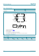
4. Functional diagram
5. Pinning information
5.1 Pinning
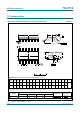
Fig 1. Logic symbol Fig 2. IEC logic symbol Fig 3. Logic diagram
mna204
1A 1Y
1
2
2A 2Y
3
4
3A 3Y
5
6
4A 4Y
9
8
5A 5Y
11
10
6A 6Y
13
12
8
9
10
11
001aac497
12
13
2
1
4
3
6
5
mna025
A
Y
(1) The die substrate is attached to this pad using a
conductive die attach material. It cannot be used as a
supply pin or input.
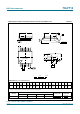
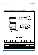
Fig 4. Pin configuration for SO14 and (T)SSOP14 Fig 5. Pin configuration for DHVQFN14
74LVT14
1A V
CC
1Y 6A
2A 6Y
2Y 5A
3A 5Y
3Y 4A
GND 4Y
001aah920
1
2
3
4
5
6
7
8
10
9
12
11
14
13
001aah921
74LVT14
GND
(1)
Transparent top view
3Y 4A
3A 5Y
2Y 5A
2A 6Y
1Y 6A
GND
4Y
1A
V
CC
6 9
5 10
4 11
3 12
2 13
7
8
1
14
terminal 1
index area