
Datasheet


74HC_HCT540 All information provided in this document is subject to legal disclaimers. © NXP B.V. 2013. All rights reserved.
Product data sheet Rev. 3 — 21 January 2013 5 of 18
NXP Semiconductors
74HC540; 74HCT540
Octal buffer/line driver; 3-state; inverting
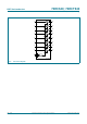
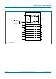
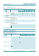
5. Pinning information
5.1 Pinning
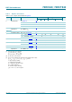
5.2 Pin description
6. Functional description
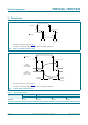
[1] H = HIGH voltage level; L = LOW voltage level; X = don’t care; Z = high-impedance OFF-state.
Fig 5. Pin configuration DIP20, SO20 and SSOP20
+&
+&7
2( 9
&&
$
2(
$
<
$
<
$
<
$
<
$
<
$
<
$
<
*1' <
DDD
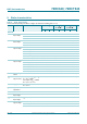
Table 2. Pin description
Symbol Pin Description
OE
1 1 output enable input (active LOW)
A0 to A7 2, 3, 4, 5, 6, 7, 8, 9 data input
GND 10 ground (0 V)
Y
0 to Y7 18, 17, 16, 15, 14, 13, 12, 11 data output
OE
2 19 output enable input (active LOW)
V
CC
20 supply voltage
Table 3. Functional table
[1]
Control Input Output
OE1 OE2 An Yn
LL L H
LL H L
XH X Z
HX X Z