
Datasheet


74HC_HCT157 All information provided in this document is subject to legal disclaimers. © NXP Semiconductors N.V. 2015. All rights reserved.
Product data sheet Rev. 7 — 21 January 2015 4 of 19
NXP Semiconductors
74HC157; 74HCT157
Quad 2-input multiplexer
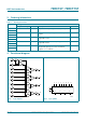
5.2 Pin description
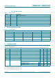
6. Functional description
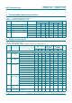
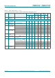
[1] H = HIGH voltage level; L = LOW voltage level; X = don’t care.
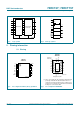
7. Limiting values
[1] P
tot
derates linearly with 8 mW/K above 70 C.
[2] P
tot
derates linearly with 5.5 mW/K above 60 C.
[3] P
tot
derates linearly with 4.5 mW/K above 60 C.
Table 2. Pin description
Symbol Pin Description
S 1 common data select input
1I0 to 4I0 2, 5, 11, 14 data inputs from source 0
1I1 to 4I1 3, 6, 10, 13 data inputs from source 1
1Y to 4Y 4, 7, 9, 12 multiplexer outputs
GND 8 ground (0 V)
E
15 enable input (active LOW)
V
CC
16 supply voltage
Table 3. Function table
[1]
Input Output
E S nI0 nI1 nY
HXXXL
LLLXL
LLHXH
LHXLL
LHXHH
Table 4. Limiting values
In accordance with the Absolute Maximum Rating System (IEC 60134). Voltages are referenced to GND (ground = 0 V).
Symbol Parameter Conditions Min Max Unit
V
CC
supply voltage 0.5 +7 V
I
IK
input clamping current V
I
< 0.5 V or V
I
>V
CC
+0.5 V - 20 mA
I
OK
output clamping current V
O
< 0.5 V or V
O
>V
CC
+0.5V - 20 mA
I
O
output current V
O
= 0.5 V to (V
CC
+0.5V) - 25 mA
I
CC
supply current - +50 mA
I
GND
ground current - 50 mA
T
stg
storage temperature 65 +150 C
P
tot
total power dissipation T
amb
= 40 C to +125 C
SO16 package
[1]
- 500 mW
(T)SSOP16 package
[2]
- 500 mW
DHVQFN16 package
[3]
- 500 mW