
Datasheet


74HC_HCT00 All information provided in this document is subject to legal disclaimers. © NXP B.V. 2011. All rights reserved.
Product data sheet Rev. 6 — 14 December 2011 2 of 16
NXP Semiconductors
74HC00; 74HCT00
Quad 2-input NAND gate
4. Functional diagram
5. Pinning information
5.1 Pinning
5.2 Pin description
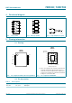
Fig 1. Logic symbol Fig 2. IEC logic symbol Fig 3. Logic diagram (one gate)
mna212
1A
1Y
1B
1
2
3
2A
2Y
2B
4
5
6
3A
3Y
3B
9
10
8
4A
4Y
4B
12
13
11
mna246
3
1
2
&
6
4
5
&
8
9
10
&
11
12
13
&
mna211
A
B
Y
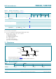
(1) This is not a supply pin. The substrate is attached to this
pad using conductive die attach material. There is no
electrical or mechanical requirement to solder this pad.
However, if it is soldered, the solder land should remain
floating or be connected to GND.
Fig 4. Pin configuration DIP14, SO14 and (T)SSOP14 Fig 5. Pin configuration DHVQFN14
74HC00
74HCT00
1A V
CC
1B 4B
1Y 4A
2A 4Y
2B 3B
2Y 3A
GND 3Y
001aal323
1
2
3
4
5
6
7 8
10
9
12
11
14
13
001aal324
74HC00
74HCT00
GND
(1)
Transparent top view
2Y 3A
2B 3B
2A 4Y
1Y 4A
1B 4B
GND
3Y
1A
V
CC
6 9
5 10
4 11
3 12
2 13
7
8
1
14
terminal 1
index area
Table 2. Pin description
Symbol Pin Description
1A to 4A 1, 4, 9, 12 data input
1B to 4B 2, 5, 10, 13 data input