
Datasheet


74HC_HCT7541 All information provided in this document is subject to legal disclaimers. © NXP B.V. 2011. All rights reserved.
Product data sheet Rev. 3 — 25 July 2011 6 of 17
NXP Semiconductors
74HC7541; 74HCT7541
Octal Schmitt trigger buffer/line driver; 3-state
[1] t
pd
is the same as t
PLH
and t
PHL
.
t
en
is the same as t
PZL
and t
PZH
.
t
dis
is the same as t
PLZ
and t
PHZ
.
[2] t
t
is the same as t
THL
and t
TLH
.
[3] C
PD
is used to determine the dynamic power dissipation (P
D
in W):
P
D
=C
PD
V
CC
2
f
i
N+ (C
L
V
CC
2
f
o
) where:
f
i
= input frequency in MHz;
f
o
= output frequency in MHz;
C
L
= output load capacitance in pF;
V
CC
= supply voltage in V;
N = number of inputs switching;
(C
L
V
CC
2
f
o
) = sum of outputs.
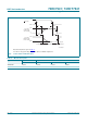
11. Waveforms
74HCT7541
t
pd
propagation delay An to Yn; see Figure 5
[1]
V
CC
= 4.5 V - 19 32 40 48 ns
V
CC
= 5.0 V; C
L
=15pF - 16 - - - ns
t
en
enable time OEn to Yn; see Figure 6
[1]
V
CC
= 4.5 V - 18 32 40 48 ns
t
dis
disable time OEn to Yn; see Figure 6
[1]
V
CC
= 4.5 V - 20 32 40 48 ns
t
t
transition time V
CC
= 4.5 V; see Figure 5
[2]
- 5 12 15 18 ns
C
PD
power dissipation
capacitance
per package;
V
I
=GNDtoV
CC
1.5 V
[3]
-32- - - pF
Table 7. Dynamic characteristics
GND = 0 V; C
L
= 50 pF; for test circuit see Figure 7.
Symbol Parameter Conditions T
amb
= 25 C T
amb
= 40 C to +125 C Unit
Min Typ Max Max (85 C) Max (125 C)
Measurement points are given in Table 8.
V
OL
and V
OH
are typical voltage output levels that occur with the output load.
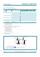
Fig 5. Input to output propagation delays
aaa-000088
V
M
V
M
90 %
10 %
Yn output
An input
V
l
GND
V
OH
V
OL
t
THL
t
TLH
t
PLH
V
M
V
M
t
PHL