
Datasheet


74HC73_4 © NXP B.V. 2008. All rights reserved.
Product data sheet Rev. 04 — 19 March 2008 8 of 16
NXP Semiconductors
74HC73
Dual JK flip-flop with reset; negative-edge trigger
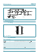
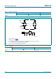
11. Waveforms
The shaded areas indicate when the input is permitted to change for predictable output performance.
Measurement points are given in Table 8.
V
OL
and V
OH
are typical voltage output levels that occur with the output load.
Fig 6. Waveforms showing the clock (nCP) to output (nQ, nQ) propagation delays, the clock pulse width, the J
and K to n
CP set-up and hold times, the output transition times and the maximum clock frequency
t
su
1/f
max
t
h
nCP input
V
M
V
M
t
h
t
su
t
W
nJ, nK
input
001aab983
nQ output
V
I
GND
90 %
10 %
10 % 10 %
10 %
90 %
90 %
90 %
V
I
V
OH
V
OL
V
OH
V
OL
GND
nQ output
t
PHL
t
PLH
V
M
t
TLH
t
THL
t
TLH
V
M
t
THL
t
PLH
t
PHL
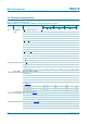
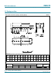
Measurement points are given in Table 8.
V
OL
and V
OH
are typical voltage output levels that occur with the output load.
Fig 7. Waveforms showing the reset (nR) input to output (nQ, nQ) propagation delays and the reset pulse width
and the n
R to nCP removal time
001aab984
nQ output
V
I
GND
V
I
GND
V
OH
V
OL
V
OH
V
OL
t
W
nR input
V
M
nQ output
nCP input
V
M
t
rec
t
PHL
t
PLH