
Datasheet


74HC73_4 © NXP B.V. 2008. All rights reserved.
Product data sheet Rev. 04 — 19 March 2008 3 of 16
NXP Semiconductors
74HC73
Dual JK flip-flop with reset; negative-edge trigger
5. Pinning information
5.1 Pinning
5.2 Pin description
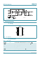
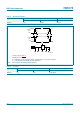
Fig 4. Logic diagram (one flip-flop)
001aab982
C
C
K
J
R
CP
C
C
C
C
C
C
C
C
Q
Q
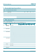
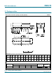
Fig 5. Pin configuration
74HC73
1CP 1J
1R 1Q
1K 1Q
V
CC
GND
2CP 2K
2R 2Q
2J 2Q
001aab978
1
2
3
4
5
6
7 8
10
9
12
11
14
13
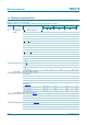
Table 2. Pin description
Symbol Pin Description
1
CP, 2CP 1, 5 clock input (HIGH-to-LOW edge-triggered); also referred to as nCP
1
R, 2R 2, 6 asynchronous reset input (active LOW); also referred to as nR
1K, 2K 3, 10 synchronous K input; also referred to as nK
V
CC
4 positive supply voltage
GND 11 ground (0 V)
1Q, 2Q 12, 9 true output; also referred to as nQ
1
Q, 2Q 13, 8 complement output; also referred to as nQ
1J, 2J 14, 7 synchronous J input; also referred to as nJ