
Datasheet
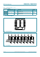
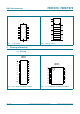

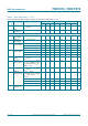
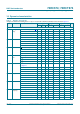

Table Of Contents
- 1. General description
- 2. Features and benefits
- 3. Ordering information
- 4. Functional diagram
- 5. Pinning information
- 6. Functional description
- 7. Limiting values
- 8. Recommended operating conditions
- 9. Static characteristics
- 10. Dynamic characteristics
- 11. Waveforms
- 12. Package outline
- 13. Abbreviations
- 14. Revision history
- 15. Legal information
- 16. Contact information
- 17. Contents
74HC_HCT574 All information provided in this document is subject to legal disclaimers. © NXP Semiconductors N.V. 2015. All rights reserved.
Product data sheet Rev. 6 — 26 January 2015 9 of 19
NXP Semiconductors
74HC574; 74HCT574
Octal D-type flip-flop; positive edge-trigger; 3-state
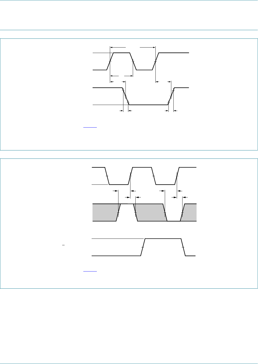
11. Waveforms
Measurement points are given in Table 8.
V
OL
and V
OH
are typical voltage output levels that occur with the output load.
Fig 7. Propagation delay input (CP) to output (Qn), output transition time, clock input (CP) pulse width and the
maximum frequency (CP)
DDQ
&3LQSXW
I
PD[
W
:
W
7+/
W
7/+
W
3+/
W
3/+
9
2+
9
,
*1'
9
2/
9
0
9
0
4QRXWSXW
Measurement points are given in Table 8.
V
OL
and V
OH
are typical voltage output levels that occur with the output load.
Fig 8. The data input (D) to clock input (CP) set-up times and clock input (CP) to data input (D) hold times
PQD
*1'
*1'
W
K
W
VX
W
K
W
VX
9
0
9
0
9
0
9
,
9
2+
9
2/
9
,
4QRXWSXW
&3LQSXW
'QLQSXW