
Datasheet
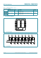
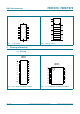

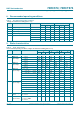
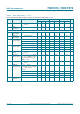
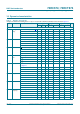

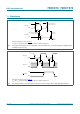
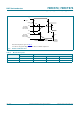
Table Of Contents
- 1. General description
- 2. Features and benefits
- 3. Ordering information
- 4. Functional diagram
- 5. Pinning information
- 6. Functional description
- 7. Limiting values
- 8. Recommended operating conditions
- 9. Static characteristics
- 10. Dynamic characteristics
- 11. Waveforms
- 12. Package outline
- 13. Abbreviations
- 14. Revision history
- 15. Legal information
- 16. Contact information
- 17. Contents
74HC_HCT574 All information provided in this document is subject to legal disclaimers. © NXP Semiconductors N.V. 2015. All rights reserved.
Product data sheet Rev. 6 — 26 January 2015 8 of 19
NXP Semiconductors
74HC574; 74HCT574
Octal D-type flip-flop; positive edge-trigger; 3-state
[1] t
pd
is the same as t
PLH
and t
PHL
.
[2] t
en
is the same as t
PZH
and t
PZL
.
[3] t
dis
is the same as t
PLZ
and t
PHZ
.
[4] t
t
is the same as t
THL
and t
TLH
.
[5] C
PD
is used to determine the dynamic power dissipation (P
D
in W).
P
D
=C
PD
V
CC
2
f
i
N+(C
L
V
CC
2
f
o
) where:
f
i
= input frequency in MHz;
f
o
= output frequency in MHz;
C
L
= output load capacitance in pF;
V
CC
= supply voltage in V;
N = number of inputs switching;
(C
L
V
CC
2
f
o
) = sum of outputs.
C
PD
power
dissipation
capacitance
C
L
=50pF;f=1 MHz;
V
I
=GNDtoV
CC
[5]
-22- - - - -pF
74HCT574
t
pd
propagation
delay
CP to Qn; see Figure 7
[1]
V
CC
= 4.5 V - 18 33 - 41 - 50 ns
V
CC
=5V; C
L
=15pF - 15 - - - - - ns
t
en
enable time OE to Qn; see Figure 9
[2]
V
CC
= 4.5 V - 19 33 - 41 - 50 ns
t
dis
disable time OE to Qn; see Figure 9
[3]
V
CC
= 4.5 V - 16 28 - 35 - 42 ns
t
t
transition
time
Qn; see Figure 7
[4]
V
CC
= 4.5 V - 5 12 - 15 - 18 ns
t
W
pulse width CP HIGH or LOW;
see Figure 8
V
CC
= 4.5 V 16 7 - 20 - 24 - ns
t
su
set-up time Dn to CP; see Figure 8
V
CC
= 4.5 V 12 3 - 15 - 18 - ns
t
h
hold time Dn to CP; see Figure 8
V
CC
= 4.5 V 5 1- 5 - 5 - ns
f
max
maximum
frequency
CP; see Figure 7
V
CC
= 4.5 V 30 69 - 24 - 20 - MHz
V
CC
=5V; C
L
=15pF - 76 - - - - - MHz
C
PD
power
dissipation
capacitance
C
L
=50pF;f=1 MHz;
V
I
=GNDtoV
CC
1.5 V
[5]
-25- - - - -pF
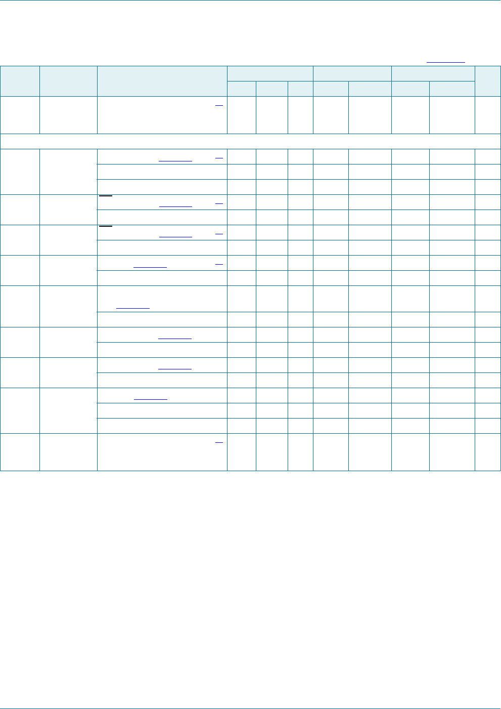
Table 7. Dynamic characteristics
…continued
Voltages are referenced to GND (ground = 0 V); C
L
= 50 pF unless otherwise specified; for test circuit see Figure 10.
Symbol Parameter Conditions 25 C 40 C to +85 C 40 C to +125 C Unit
Min Typ Max Min Max Min Max