
Datasheet
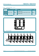
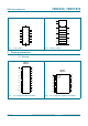

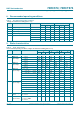
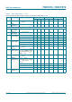
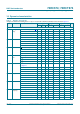

Table Of Contents
- 1. General description
- 2. Features and benefits
- 3. Ordering information
- 4. Functional diagram
- 5. Pinning information
- 6. Functional description
- 7. Limiting values
- 8. Recommended operating conditions
- 9. Static characteristics
- 10. Dynamic characteristics
- 11. Waveforms
- 12. Package outline
- 13. Abbreviations
- 14. Revision history
- 15. Legal information
- 16. Contact information
- 17. Contents
74HC_HCT574 All information provided in this document is subject to legal disclaimers. © NXP Semiconductors N.V. 2015. All rights reserved.
Product data sheet Rev. 6 — 26 January 2015 4 of 19
NXP Semiconductors
74HC574; 74HCT574
Octal D-type flip-flop; positive edge-trigger; 3-state
5.2 Pin description
6. Functional description
[1] H = HIGH voltage level;
h = HIGH voltage level one setup time prior to the HIGH-to-LOW CP transition;
L = LOW voltage level;
l = LOW voltage level one setup time prior to the HIGH-to-LOW CP transition;
Z = high-impedance OFF-state;
= LOW-to-HIGH clock transition.
7. Limiting values
[1] For DIP20 package: P
tot
derates linearly with 12 mW/K above 70 C.
[2] For SO20: P
tot
derates linearly with 8 mW/K above 70 C.
For SSOP20 and TSSOP20 packages: P
tot
derates linearly with 5.5 mW/K above 60 C.
Table 2. Pin description
Symbol Pin Description
OE
1 3-state output enable input (active LOW)
D[0:7] 2, 3, 4, 5, 6, 7, 8, 9 data input
GND 10 ground (0 V)
CP 11 clock input (LOW-to-HIGH, edge triggered)
Q[0:7] 19, 18, 17, 16, 15, 14, 13, 12 3-state flip-flop output
V
CC
20 supply voltage
Table 3. Function table
[1]
Operating mode Input Internal
flip-flop
Output
OE CP Dn Qn
Load and read register L lL L
L hH H
Load register and disable output H lL Z
H hH Z
Table 4. Limiting values
In accordance with the Absolute Maximum Rating System (IEC 60134). Voltages are referenced to GND (ground = 0 V).
Symbol Parameter Conditions Min Max Unit
V
CC
supply voltage 0.5 +7 V
I
IK
input clamping current V
I
< 0.5 V or V
I
>V
CC
+0.5 V - 20 mA
I
OK
output clamping current V
O
< 0.5 V or V
O
>V
CC
+0.5V - 20 mA
I
O
output current V
O
= 0.5 V to (V
CC
+0.5V) - 35 mA
I
CC
supply current - +70 mA
I
GND
ground current - 70 mA
T
stg
storage temperature 65 +150 C
P
tot
total power dissipation DIP20 package
[1]
- 750 mW
SO20, SSOP20 and TSSOP20 packages
[2]
- 500 mW