
Datasheet


74HC_HCT4066_Q100 All information provided in this document is subject to legal disclaimers. © NXP B.V. 2013. All rights reserved.
Product data sheet Rev. 3 — 16 December 2013 9 of 23
NXP Semiconductors
74HC4066-Q100; 74HCT4066-Q100
Quad single-pole single-throw analog switch
10. Dynamic characteristics
[1] Typical values are measured at T
amb
= 25 C.
[2] t
pd
is the same as t
PHL
and t
PLH
.
[3] t
on
is the same as t
PHZ
and t
PLZ
.
[4] t
off
is the same as t
PZH and
t
PZL
.
[5] C
PD
is used to determine the dynamic power dissipation (P
D
in W).
P
D
= C
PD
V
CC
2
f
i
+ {(C
L
+C
sw
) V
CC
2
f
o
} where:
f
i
= input frequency in MHz;
f
o
= output frequency in MHz;
{(C
L
+C
sw
) V
CC
2
f
o
} = sum of outputs;
C
L
= output load capacitance in pF;
C
sw
= switch capacitance in pF;
V
CC
= supply voltage in V.
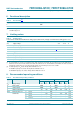
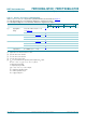
Table 9. Dynamic characteristics 74HC4066-Q100
GND = 0 V; t
r
= t
f
= 6 ns; C
L
= 50 pF unless specified otherwise; for test circuit see Figure 12.
V
is
is the input voltage at a Yn or Z terminal, whichever is assigned as an input.
V
os
is the output voltage at a Yn or Z terminal, whichever is assigned as an output.
Symbol Parameter Conditions 40 C to +85 C 40 C to +125 C Unit
Min Typ
[1]
Max Min Max
t
pd
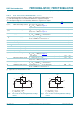
propagation delay nY to nZ or nZ to nY; R
L
= ;
see Figure 10
[2]
V
CC
= 2.0 V - 8 75 - 90 ns
V
CC
= 4.5 V - 3 15 - 18 ns
V
CC
= 6.0 V - 2 13 - 15 ns
V
CC
= 9.0 V - 2 10 - 12 ns
t
off
turn-off time nE to nY or nZ; see Figure 11
[4]
V
CC
= 2.0 V - 44 190 - 225 ns
V
CC
= 4.5 V - 16 38 - 45 ns
V
CC
= 5.0 V; C
L
= 15 pF - 13 - - - ns
V
CC
= 6.0 V - 13 33 - 38 ns
V
CC
= 9.0 V - 16 26 - 30 ns
t
on
turn-on time nE to nY or nZ; see Figure 11
[3]
V
CC
= 2.0 V - 36 125 - 150 ns
V
CC
= 4.5 V - 13 25 - 30 ns
V
CC
= 5.0 V; C
L
= 15 pF - 11 - - - ns
V
CC
= 6.0 V - 10 21 - 26 ns
V
CC
= 9.0 V - 8 16 - 20 ns
C
PD
power dissipation
capacitance
per switch; V
I
= GND to V
CC
[5]
11 - - - pF