
Datasheet


74HC_HCT4066_Q100 All information provided in this document is subject to legal disclaimers. © NXP B.V. 2013. All rights reserved.
Product data sheet Rev. 3 — 16 December 2013 6 of 23
NXP Semiconductors
74HC4066-Q100; 74HCT4066-Q100
Quad single-pole single-throw analog switch
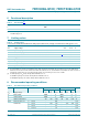
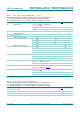
V
is
= 0 V to V
CC
V
is
= 0 V to V
CC
Fig 6. Test circuit for measuring R
ON
Fig 7. Typical R
ON
as a function of input voltage V
is
aaa-003458
V
is
I
SW
V
IH
V
CC
GND
nZnY
nE
V
SW
V
is
(V)
0 9.07.23.6 5.41.8
aaa-003459
30
40
20
50
60
R
ON
(Ω)
10
V
CC
= 4.5 V
6 V
9 V
R
ON
V
SW
I
SW
----------
=
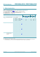
Table 7. Static characteristics 74HC4066-Q100
At recommended operating conditions; voltages are referenced to GND (ground = 0 V).
V
is
is the input voltage at a Yn or Z terminal, whichever is assigned as an input.
V
os
is the output voltage at a Yn or Z terminal, whichever is assigned as an output.
Symbol Parameter Conditions Min Typ
[1]
Max Unit
T
amb
= 40 C to +85 C
V
IH
HIGH-level input voltage V
CC
= 2.0 V 1.5 1.2 - V
V
CC
= 4.5 V 3.15 2.4 - V
V
CC
= 6.0 V 4.2 3.2 - V
V
CC
= 9.0 V 6.3 4.7 - V
V
IL
LOW-level input voltage V
CC
= 2.0 V - 0.8 0.5 V
V
CC
= 4.5 V - 2.1 1.35 V
V
CC
= 6.0 V - 2.8 1.80 V
V
CC
= 9.0 V - 4.3 2.70 V
I
I
input leakage current V
I
= V
CC
or GND
V
CC
= 6.0 V - - 1.0 A
V
CC
= 10.0 V - - 2.0 A
I
S(OFF)
OFF-state leakage current V
CC
= 10.0 V; V
I
= V
IH
or V
IL
;
V
SW
=V
CC
GND; see Figure 8
per channel - - 1.0 A
I
S(ON)
ON-state leakage current V
CC
= 10.0 V; V
I
= V
IH
or V
IL
;
V
SW
=V
CC
GND; see Figure 9
--1.0 A