
Datasheet


74HC_HCT4066_Q100 All information provided in this document is subject to legal disclaimers. © NXP B.V. 2013. All rights reserved.
Product data sheet Rev. 3 — 16 December 2013 5 of 23
NXP Semiconductors
74HC4066-Q100; 74HCT4066-Q100
Quad single-pole single-throw analog switch
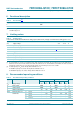
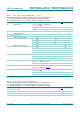
9. Static characteristics
[1] Typical values are measured at T
amb
= 25 C.
[2] At supply voltages (V
CC
GND) approaching 2 V, the analog switch ON resistance becomes extremely non-linear. Therefore it is
recommended that these devices be used to transmit digital signals only, when using these supply voltages.
Table 6. R
ON
resistance per switch for types 74HC4066-Q100 and 74HCT4066-Q100
V
I
= V
IH
or V
IL
; for test circuit see Figure 6.
V
is
is the input voltage at a Yn or Z terminal, whichever is assigned as an input.
V
os
is the output voltage at a Yn or Z terminal, whichever is assigned as an output.
For 74HC4066-Q100: V
CC
GND = 2.0 V, 4.5 V, 6.0 V and 9.0 V.
For 74HCT4066-Q100: V
CC
GND = 4.5 V.
Symbol Parameter Conditions 40 C to +85 C 40 C to +125
C
Unit
Min Typ
[1]
Max Min Max
R
ON(peak)
ON resistance (peak) V
is
= V
CC
to GND
V
CC
= 2.0 V; I
SW
= 100 A
[2]
-----
V
CC
= 4.5 V; I
SW
= 1000 A - 54 - 118 142
V
CC
= 6.0 V; I
SW
= 1000 A - 42 - 105 126
V
CC
= 9.0 V; I
SW
= 1000 A - 32 - 88 105
R
ON(rail)
ON resistance (rail) V
is
= GND
V
CC
= 2.0 V; I
SW
= 100 A
[2]
-80---
V
CC
= 4.5 V; I
SW
= 1000 A - 35 - 95 115
V
CC
= 6.0 V; I
SW
= 1000 A - 27 - 82 100
V
CC
= 9.0 V; I
SW
= 1000 A-20-7085
V
is
= V
CC
V
CC
= 2.0 V; I
SW
= 100 A
[2]
-100---
V
CC
= 4.5 V; I
SW
= 1000 A - 42 - 106 128
V
CC
= 6.0 V; I
SW
= 1000 A - 35 - 94 113
V
CC
= 9.0 V; I
SW
= 1000 A-20-7895
R
ON
ON resistance
mismatch between
channels
V
is
= V
CC
to GND
V
CC
= 2.0 V
[2]
-----
V
CC
= 4.5V -5---
V
CC
= 6.0V -4---
V
CC
= 9.0V -3---