
Datasheet


74HC_HCT4066_Q100 All information provided in this document is subject to legal disclaimers. © NXP B.V. 2013. All rights reserved.
Product data sheet Rev. 3 — 16 December 2013 3 of 23
NXP Semiconductors
74HC4066-Q100; 74HCT4066-Q100
Quad single-pole single-throw analog switch
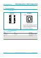
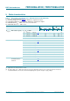
5. Pinning information
5.1 Pinning
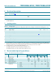
5.2 Pin description
(1) This is not a supply pin. The substrate is attached to this
pad using conductive die attach material. There is no
electrical or mechanical requirement to solder this pad.
However, if it is soldered, the solder land should remain
floating or be connected to VCC.
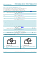
Fig 4. Pin configuration for SO14 and TSSOP14 Fig 5. Pin configuration for DHVQFN14
+&4
+&74
< 9
&&
= (
= (
< <
( =
( =
*1' <
DDD
DDD
+&4
+&74
7UDQVSDUHQWWRSYLHZ
( =
( =
< <
= (
= (
*1'
<
<
9
&&
WHUPLQDO
LQGH[DUHD
9
&&
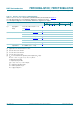
Table 2. Pin description
Symbol Pin Description
1Z, 2Z, 3Z, 4Z 2, 3, 9, 10 independent input or output
1Y, 2Y, 3Y, 4Y 1, 4, 8, 11 independent input or output
GND 7 ground (0 V)
1E, 2E, 3E, 4E 13, 5, 6, 12 enable input (active HIGH)
V
CC
14 supply voltage