74HC4066-Q100; 74HCT4066-Q100 Quad single-pole single-throw analog switch Rev. 3 — 16 December 2013 Product data sheet 1. General description The 74HC4066-Q100; 74HCT4066-Q100 is a quad single pole, single throw analog switch. Each switch features two input/output terminals (nY and nZ) and an active HIGH enable input (nE). When nE is LOW, the analog switch is turned off. Inputs include clamp diodes. This enables the use of current limiting resistors to interface inputs to voltages in excess of VCC.
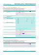
74HC4066-Q100; 74HCT4066-Q100 NXP Semiconductors Quad single-pole single-throw analog switch 3. Ordering information Table 1. Ordering information Type number Package 74HC4066D-Q100 Temperature range Name Description Version 40 C to +125 C SO14 plastic small outline package; 14 leads; body width 3.9 mm SOT108-1 40 C to +125 C TSSOP14 plastic thin shrink small outline package; 14 leads; body width 4.
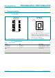
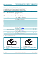
74HC4066-Q100; 74HCT4066-Q100 NXP Semiconductors Quad single-pole single-throw analog switch 5. Pinning information 5.1 Pinning < WHUPLQDO LQGH[ DUHD 9&& +& 4 +&7 4 +& 4 +&7 4 9&& = ( = ( = ( < < ( = ( = *1' < < ( ( < 9&& = < ( < *1' = = DDD 7UDQVSDUHQW WRS YLHZ DDD (1) This is not a supply pin.
NXP Semiconductors 74HC4066-Q100; 74HCT4066-Q100 Quad single-pole single-throw analog switch 6. Functional description Table 3. Function table[1] Input nE Switch L OFF H ON [1] H = HIGH voltage level; L = LOW voltage level. 7. Limiting values Table 4. Limiting values In accordance with the Absolute Maximum Rating System (IEC 60134). Voltages are referenced to GND (ground = 0 V). Symbol Parameter VCC supply voltage Conditions IIK input clamping current VI < 0.5 V or VI > VCC + 0.
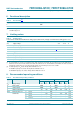
74HC4066-Q100; 74HCT4066-Q100 NXP Semiconductors Quad single-pole single-throw analog switch 9. Static characteristics Table 6. RON resistance per switch for types 74HC4066-Q100 and 74HCT4066-Q100 VI = VIH or VIL; for test circuit see Figure 6. Vis is the input voltage at a Yn or Z terminal, whichever is assigned as an input. Vos is the output voltage at a Yn or Z terminal, whichever is assigned as an output. For 74HC4066-Q100: VCC GND = 2.0 V, 4.5 V, 6.0 V and 9.0 V. For 74HCT4066-Q100: VCC GND = 4.
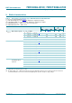
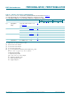
74HC4066-Q100; 74HCT4066-Q100 NXP Semiconductors Quad single-pole single-throw analog switch aaa-003459 60 RON (Ω) VCC = 4.5 V 50 VSW 6V 40 9V VCC 30 nE VIH nY Vis nZ 20 GND ISW 10 0 1.8 3.6 5.4 7.2 aaa-003458 Vis = 0 V to VCC R ON Fig 6. Vis (V) 9.0 Vis = 0 V to VCC V SW = ---------I SW Test circuit for measuring RON Fig 7. Typical RON as a function of input voltage Vis Table 7.
NXP Semiconductors 74HC4066-Q100; 74HCT4066-Q100 Quad single-pole single-throw analog switch Table 7. Static characteristics 74HC4066-Q100 …continued At recommended operating conditions; voltages are referenced to GND (ground = 0 V). Vis is the input voltage at a Yn or Z terminal, whichever is assigned as an input. Vos is the output voltage at a Yn or Z terminal, whichever is assigned as an output. Min Typ[1] Max Unit VCC = 6.0 V - - 20.0 A VCC = 10.0 V - - 40.
74HC4066-Q100; 74HCT4066-Q100 NXP Semiconductors Quad single-pole single-throw analog switch Table 8. Static characteristics 74HCT4066-Q100 …continued At recommended operating conditions; voltages are referenced to GND (ground = 0 V). Vis is the input voltage at a Yn or Z terminal, whichever is assigned as an input. Vos is the output voltage at a Yn or Z terminal, whichever is assigned as an output. Symbol Parameter Conditions IS(OFF) OFF-state leakage current VCC = 5.
74HC4066-Q100; 74HCT4066-Q100 NXP Semiconductors Quad single-pole single-throw analog switch 10. Dynamic characteristics Table 9. Dynamic characteristics 74HC4066-Q100 GND = 0 V; tr = tf = 6 ns; CL = 50 pF unless specified otherwise; for test circuit see Figure 12. Vis is the input voltage at a Yn or Z terminal, whichever is assigned as an input. Vos is the output voltage at a Yn or Z terminal, whichever is assigned as an output.
74HC4066-Q100; 74HCT4066-Q100 NXP Semiconductors Quad single-pole single-throw analog switch Table 10. Dynamic characteristics 74HCT4066-Q100 GND = 0 V; tr = tf = 6 ns; CL = 50 pF unless specified otherwise; for test circuit see Figure 12. Vis is the input voltage at a Yn or Z terminal, whichever is assigned as an input. Vos is the output voltage at a Yn or Z terminal, whichever is assigned as an output.
74HC4066-Q100; 74HCT4066-Q100 NXP Semiconductors Quad single-pole single-throw analog switch 11. Waveforms 50 % Vis input tPLH tPHL 50 % Vos output 001aad555 Fig 10. Input (Vis) to output (Vos) propagation delays VI VM E input 0V tPLZ tPZL 50 % Vos output 10 % tPHZ tPZH 90 % 50 % Vos output switch ON switch ON switch OFF aaa-003460 Measurement points are shown in Table 11. Fig 11. Turn-on and turn-off times Table 11. Measurement points Type VI 74HC4066-Q100 VCC 0.
74HC4066-Q100; 74HCT4066-Q100 NXP Semiconductors Quad single-pole single-throw analog switch VI tW 90 % negative pulse VM 0V tf tr tr tf VI 90 % positive pulse 0V VM 10 % VM VM 10 % tW VCC Vis PULSE GENERATOR VCC Vos VI S1 RL open DUT RT CL GND 001aag732 Test data is given in Table 12. Definitions test circuit: RT = Termination resistance should be equal to output impedance Zo of the pulse generator. CL = Load capacitance including jig and probe capacitance. RL = Load resistor.
74HC4066-Q100; 74HCT4066-Q100 NXP Semiconductors Quad single-pole single-throw analog switch 12. Additional dynamic characteristics Table 13. Additional dynamic characteristics Recommended conditions and typical values; GND = 0 V; Tamb = 25 C. Vis is the input voltage at a Yn or Z terminal, whichever is assigned as an input. Vos is the output voltage at a Yn or Z terminal, whichever is assigned as an output.
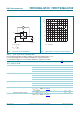
74HC4066-Q100; 74HCT4066-Q100 NXP Semiconductors Quad single-pole single-throw analog switch mna082 0 (dB) −20 −40 −60 −80 −100 10 102 103 104 105 106 fi (kHz) a. Isolation (OFF-state) VCC VCC nE VIL 2RL 0.1 μF nY/nZ fi nZ/nY VO CL 2RL dB 001aaj470 b. Test circuit VCC = 4.5 V; GND = 0 V; RL = 600 ; Rsource = 1 k. Fig 14.
74HC4066-Q100; 74HCT4066-Q100 NXP Semiconductors Quad single-pole single-throw analog switch mna083 5 (dB) 0 −5 10 102 103 104 105 106 fi (kHz) a. Typical 3 dB frequency response VCC VCC nE VIH 2RL 0.1 μF nY/nZ fi nZ/nY VO 2RL CL dB 001aaj469 b. Test circuit VCC = 4.5 V; GND = 0 V; RL = 50 ; Rsource = 1 k. Fig 15. 3 dB frequency response 74HC_HCT4066_Q100 Product data sheet All information provided in this document is subject to legal disclaimers. Rev.
74HC4066-Q100; 74HCT4066-Q100 NXP Semiconductors Quad single-pole single-throw analog switch VCC nE VCC VCC GND 2RL 2RL nY/nZ nZ/nY DUT 2RL 2RL oscilloscope CL GND mnb011 a. Circuit V(p−p) mnb012 b. Crosstalk voltage Fig 16. Test circuit for measuring crosstalk voltage (between the digital input and the switch) VCC 1E VIH 0.
74HC4066-Q100; 74HCT4066-Q100 NXP Semiconductors Quad single-pole single-throw analog switch 13. Package outline SO14: plastic small outline package; 14 leads; body width 3.9 mm SOT108-1 D E A X c y HE v M A Z 8 14 Q A2 A (A 3) A1 pin 1 index θ Lp 1 L 7 e detail X w M bp 0 2.5 5 mm scale DIMENSIONS (inch dimensions are derived from the original mm dimensions) UNIT A max. A1 A2 A3 bp c D (1) E (1) e HE L Lp Q v w y Z (1) mm 1.75 0.25 0.10 1.45 1.25 0.25 0.
74HC4066-Q100; 74HCT4066-Q100 NXP Semiconductors Quad single-pole single-throw analog switch TSSOP14: plastic thin shrink small outline package; 14 leads; body width 4.4 mm SOT402-1 E D A X c y HE v M A Z 8 14 Q (A 3) A2 A A1 pin 1 index θ Lp L 1 7 e detail X w M bp 0 2.5 5 mm scale DIMENSIONS (mm are the original dimensions) UNIT A max. A1 A2 A3 bp c D (1) E (2) e HE L Lp Q v w y Z (1) θ mm 1.1 0.15 0.05 0.95 0.80 0.25 0.30 0.19 0.2 0.1 5.1 4.9 4.5 4.
74HC4066-Q100; 74HCT4066-Q100 NXP Semiconductors Quad single-pole single-throw analog switch DHVQFN14: plastic dual in-line compatible thermal enhanced very thin quad flat package; no leads; SOT762-1 14 terminals; body 2.5 x 3 x 0.85 mm A B D A A1 E c detail X terminal 1 index area terminal 1 index area C e1 e 2 6 y y1 C v M C A B w M C b L 1 7 Eh e 14 8 13 9 Dh X 0 2.5 5 mm scale DIMENSIONS (mm are the original dimensions) UNIT mm A(1) max. A1 b 1 0.05 0.00 0.30 0.
74HC4066-Q100; 74HCT4066-Q100 NXP Semiconductors Quad single-pole single-throw analog switch 14. Abbreviations Table 14. Abbreviations Acronym Description CMOS Complementary Metal Oxide Semiconductor ESD ElectroStatic Discharge HBM Human Body Model MM Machine Model CDM Charge-Device Model MIL Military 15. Revision history Table 15. Revision history Document ID Release date 74HC_HCT4066_Q100 v.
NXP Semiconductors 74HC4066-Q100; 74HCT4066-Q100 Quad single-pole single-throw analog switch 16. Legal information 16.1 Data sheet status Document status[1][2] Product status[3] Definition Objective [short] data sheet Development This document contains data from the objective specification for product development. Preliminary [short] data sheet Qualification This document contains data from the preliminary specification.
NXP Semiconductors 74HC4066-Q100; 74HCT4066-Q100 Quad single-pole single-throw analog switch No offer to sell or license — Nothing in this document may be interpreted or construed as an offer to sell products that is open for acceptance or the grant, conveyance or implication of any license under any copyrights, patents or other industrial or intellectual property rights. Translations — A non-English (translated) version of a document is for reference only.
NXP Semiconductors 74HC4066-Q100; 74HCT4066-Q100 Quad single-pole single-throw analog switch 18. Contents 1 2 3 4 5 5.1 5.2 6 7 8 9 10 11 12 13 14 15 16 16.1 16.2 16.3 16.4 17 18 General description . . . . . . . . . . . . . . . . . . . . . . 1 Features and benefits . . . . . . . . . . . . . . . . . . . . 1 Ordering information . . . . . . . . . . . . . . . . . . . . . 2 Functional diagram . . . . . . . . . . . . . . . . . . . . . . 2 Pinning information . . . . . . . . . . . . . . . . . . . . . .