
Datasheet


74HC_HCT4002 All information provided in this document is subject to legal disclaimers. © NXP B.V. 2012. All rights reserved.
Product data sheet Rev. 4 — 17 September 2012 7 of 16
NXP Semiconductors
74HC4002; 74HCT4002
Dual 4-input NOR gate
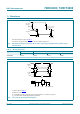
11. Waveforms
Measurement points are given in Table 8.
V
OL
and V
OH
are typical voltage output levels that occur with the output load.
Fig 7. Waveforms showing the input (nA, nB, nC, nD) to output (nY) propagation delays and the output
transition times
Q$
Q%Q&
Q'
LQSXW
Q<
RXWSXW
9
0
9
;
9
,
W
7+/
W
7/+
9
2+
9
0
9
<
9
2/
*1'
DDD
W
3+/
W
3/+
Table 8. Measurement points
Type Input Output
V
M
V
M
V
X
V
Y
74HC4002 0.5V
CC
0.5V
CC
0.1V
CC
0.9V
CC
74HCT40021.3V1.3V0.1V
CC
0.9V
CC
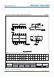
Test data is given in Table 9.
Definitions test circuit:
R
T
= termination resistance should be equal to output impedance Z
o
of the pulse generator.
C
L
= load capacitance including jig and probe capacitance.
Fig 8. Test circuit for measuring switching times
001aah768
t
W
t
W
t
r
t
r
t
f
V
M
V
I
negative
pulse
GND
V
I
positive
pulse
GND
10 %
90 %
90 %
10 %
V
M
V
M
V
M
t
f
V
CC
DUT
R
T
V
I
V
O
C
L
G