
Datasheet


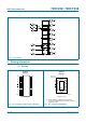

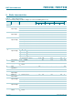
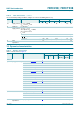
Table Of Contents
- 1. General description
- 2. Features
- 3. Ordering information
- 4. Functional diagram
- 5. Pinning information
- 6. Functional description
- 7. Limiting values
- 8. Recommended operating conditions
- 9. Static characteristics
- 10. Dynamic characteristics
- 11. Waveforms
- 12. Package outline
- 13. Abbreviations
- 14. Revision history
- 15. Legal information
- 16. Contact information
- 17. Contents

74HC_HCT238_3 © NXP B.V. 2007. All rights reserved.
Product data sheet Rev. 03 — 16 July 2007 5 of 18
NXP Semiconductors
74HC238; 74HCT238
3-to-8 line decoder/demultiplexer
7. Limiting values
[1] The input and output voltage ratings may be exceeded if the input and output current ratings are observed.
[2] For DIP16 packages: above 70 °C the value of P
tot
derates linearly at 12 mW/K.
[3] For SO16 packages: above 70 °C the value of P
tot
derates linearly at 8 mW/K.
For SSOP16 and TSSOP16 packages: above 60 °C the value of P
tot
derates linearly at 5.5 mW/K.
For DHVQFN16 packages: above 60 °C the value of P
tot
derates linearly at 4.5 mW/K.
8. Recommended operating conditions
Table 4. Limiting values
In accordance with the Absolute Maximum Rating System (IEC 60134). Voltages are referenced to GND (ground = 0 V).
Symbol Parameter Conditions Min Max Unit
V
CC
supply voltage −0.5 +7 V
I
IK
input clamping current V
I
< −0.5 V or V
I
>V
CC
+ 0.5 V
[1]
- ±20 mA
I
OK
output clamping current V
O
< −0.5 V or V
O
>V
CC
+ 0.5 V
[1]
- ±20 mA
I
O
output current −0.5 V < V
O
< V
CC
+ 0.5 V - ±25 mA
I
CC
supply current - 50 mA
I
GND
ground current −50 - mA
T
stg
storage temperature −65 +150 °C
P
tot
total power dissipation DIP16 package
[2]
- 750 mW
SO16, SSOP16, TSSOP16 and
DHVQFN16 packages
[3]
- 500 mW
Table 5. Recommended operating conditions
Voltages are referenced to GND (ground = 0 V).
Symbol Parameter Conditions 74HC238 74HCT238 Unit
Min Typ Max Min Typ Max
V
CC
supply voltage 2.0 5.0 6.0 4.5 5.0 5.5 V
V
I
input voltage 0 - V
CC
0-V
CC
V
V
O
output voltage 0 - V
CC
0-V
CC
V
T
amb
ambient temperature −40 - +125 −40 - +125 °C
∆t/∆V input transition rise
and fall rate
V
CC
= 2.0 V - - 625 - - - ns/V
V
CC
= 4.5 V - 1.67 139 - 1.67 139 ns/V
V
CC
= 6.0 V - - 83 - - - ns/V