
Datasheet


74HC237 All information provided in this document is subject to legal disclaimers. © NXP B.V. 2012. All rights reserved.
Product data sheet Rev. 6 — 23 August 2012 7 of 17
NXP Semiconductors
74HC237
3-to-8 line decoder, demultiplexer with address latches
[1] t
pd
is the same as t
PLH
and t
PHL
.
[2] t
t
is the same as t
THL
and t
TLH
.
[3] C
PD
is used to determine the dynamic power dissipation (P
D
in W).
P
D
=C
PD
V
CC
2
f
i
N+(C
L
V
CC
2
f
o
) where:
f
i
= input frequency in MHz;
f
o
= output frequency in MHz;
C
L
= output load capacitance in pF;
V
CC
= supply voltage in V;
N = number of inputs switching;
(C
L
V
CC
2
f
o
) = sum of outputs.
11. Waveforms
t
W
pulse width LE HIGH; see Figure 9
V
CC
= 2.0 V 50 11 - 65 - 75 - ns
V
CC
= 4.5 V 10 4 - 13 - 15 - ns
V
CC
= 6.0 V 9 3 - 11 - 13 - ns
t
su
set-up time An to LE; see Figure 9
V
CC
= 2.0 V 50 6 - 65 - 75 - ns
V
CC
= 4.5 V 10 2 - 13 - 15 - ns
V
CC
= 6.0 V 9 2 - 11 - 13 - ns
t
h
hold time An to LE; see Figure 9 -
V
CC
= 2.0 V 30 3 - 40 - 45 - ns
V
CC
= 4.5 V 6 1 - 8 - 9 - ns
V
CC
= 6.0 V 5 1 - 7 - 8 - ns
C
PD
power
dissipation
capacitance
C
L
=50pF;f=1 MHz;
V
I
=GNDtoV
CC
[3]
-60- - - - -pF
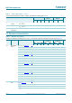
Table 7. Dynamic characteristics
…continued
Voltages are referenced to GND (ground = 0 V); C
L
= 50 pF unless otherwise specified; for test circuit see Figure 10.
Symbol Parameter Conditions T
amb
= 25 C T
amb
= 40 C
to +85 C
T
amb
= 40 C
to +125 C
Unit
Min Typ Max Min Max Min Max
Measurement points are given in Table 8.
V
OL
and V
OH
are typical voltage output levels that occur with the output load.
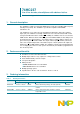
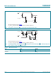
Fig 7. Propagation delay input (An) and enable inputs (E2, LE) to output (Yn) and output transition time
001aab873
An, E2, LE
input
Yn output
V
M
t
PHL
t
THL
t
TLH
t
PLH
V
M
90 %90 %
10 %10 %