
Datasheet


74HC237 All information provided in this document is subject to legal disclaimers. © NXP B.V. 2012. All rights reserved.
Product data sheet Rev. 6 — 23 August 2012 4 of 17
NXP Semiconductors
74HC237
3-to-8 line decoder, demultiplexer with address latches
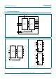
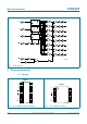
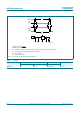
5.2 Pin description
6. Functional description
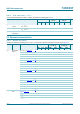
[1] H = HIGH voltage level; L = LOW voltage level; X = don’t care; Z = high-impedance OFF-state.
7. Limiting values
Table 2. Pin description
Symbol Pin Description
A0 to A2 1, 2, 3 data input
LE
4 latch enable input (active LOW)
E
1 5 data enable input 1 (active LOW)
E2 6 data enable input 2 (active HIGH)
Y0 to Y7 15, 14, 13, 12, 11, 10, 9, 7 output
GND 8 ground (0 V)
V
CC
16 supply voltage
Table 3: Function table
Enable Input Output
LE E1 E2 A0 A1 A2 Y0 Y1 Y2 Y3 Y4 Y5 Y6 Y7
HL HXXXstable
XHXXXXLLLLLLLL
XXLXXXLLLLLLLL
LLHLLLHLLLLLLL
HLLLHLLLLLL
LHLLLHLLLLL
HHLLLLHLLLL
LLHLLLLHLLL
HL HL L L L L HL L
LHHLLLLLLHL
HHHLLLLLLLH
Table 4. Limiting values
In accordance with the Absolute Maximum Rating System (IEC 60134). Voltages are referenced to GND (ground = 0 V).
Symbol Parameter Conditions Min Max Unit
V
CC
supply voltage 0.5 +7 V
I
IK
input clamping current V
I
< 0.5 V or V
I
>V
CC
+0.5 V - 20 mA
I
OK
output clamping current V
O
< 0.5 V or V
O
>V
CC
+0.5V - 20 mA
I
O
output current V
O
= 0.5 V to (V
CC
+0.5V) - 25 mA
I
CC
supply current - +50 mA
I
GND
ground current - 50 mA
T
stg
storage temperature 65 +150 C
P
tot
total power dissipation DIP16 package
[1]
- 750 mW
SO16 and SSOP16 packages
[2]
- 500 mW