
User's Guide
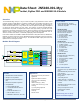
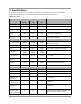
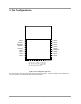
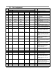
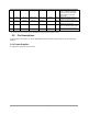
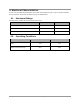
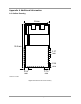
Table Of Contents
- 1. Introduction
- 2. Specifications
- 3. Pin Configurations
- 4. Electrical Characteristics
- Appendix A Additional Information
- A.1 Outline Drawing
- A.2 Module PCB Footprint
- A.3 Optimal PCB placement of the JN5168-001-M00 Module
- A.4 JN5168-001-M00 Antenna Radiation Pattern
- A.5 Manufacturing
- A.5.1 Reflow Profile
- A.5.2 Soldering Paste and Cleaning
- A.6 Ordering Information
- A.7 Related Documents
- A.8 Federal Communication Commission Interference Statement
- A.8.1 Antennas approved by FCC for use with JN5168 modules
- A.8.2 High Power Module usage limitation
- A.8.3 FCC End Product Labelling
- A.9 Industry Canada Statement
- A.9.1 Industry Canada End Product Labelling
- A.10 European R & TTE Directive 1999/5/EC Statement
- A.11 RoHS Compliance
- A.12 Status Information
- A.13 Disclaimers
- Version Control

© NXP Laboratories UK 2012 JN-DS-JN5168-001-Myy 1v0 9
4. Electrical Characteristics
In most cases, the Electrical Characteristics are the same for both module and chip. They are described in detail in
the chip datasheet. Where there are differences, they are detailed below.
4.1. Maximum Ratings
Exceeding these conditions will result in damage to the device.
Parameter Min Max
Device supply voltage VDD
-0.3V
3.6V
All Pins
-0.3V
VDD + 0.3V
Storage temperature
-40ºC
150ºC
4.2. Operating Conditions
Supply Min Max
VDD 2.0V 3.6V
Ambient temperature range -40ºC 85ºC