
User's Guide
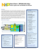
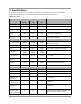
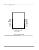
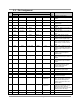
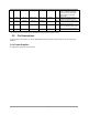
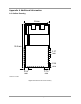
Table Of Contents
- 1. Introduction
- 2. Specifications
- 3. Pin Configurations
- 4. Electrical Characteristics
- Appendix A Additional Information
- A.1 Outline Drawing
- A.2 Module PCB Footprint
- A.3 Optimal PCB placement of the JN5168-001-M00 Module
- A.4 JN5168-001-M00 Antenna Radiation Pattern
- A.5 Manufacturing
- A.5.1 Reflow Profile
- A.5.2 Soldering Paste and Cleaning
- A.6 Ordering Information
- A.7 Related Documents
- A.8 Federal Communication Commission Interference Statement
- A.8.1 Antennas approved by FCC for use with JN5168 modules
- A.8.2 High Power Module usage limitation
- A.8.3 FCC End Product Labelling
- A.9 Industry Canada Statement
- A.9.1 Industry Canada End Product Labelling
- A.10 European R & TTE Directive 1999/5/EC Statement
- A.11 RoHS Compliance
- A.12 Status Information
- A.13 Disclaimers
- Version Control

8 JN-DS-JN5168-001-Myy 1v0 © NXP Laboratories UK 2012
SPISSEL
UART 0 Transmit Data Output,
UART 1 Transmit Data Output,
JTAG Data Output, SPI Master
Select Output 1 or SPI Slave
Select Input
24
DIO15 SIF_D RXD0 RXD1 JTAG_TDI SPISEL2
CMOS
DIO15, Serial Interface Data or
Intelligent Peripheral Data Out
25
DIO16 COMP1P SIF_CLK SPISMOSI
CMOS
DIO16, Comparator Positive Input,
Serial Interface clock or SPI Slave
Master Out Slave In Input
26 DIO17 COMP1M PWM4 I2C DATA SPISIMO CMOS
DIO17, Comparator Negative
Input, Serial Interface Data or SPI
Slave Master In Slave Out Output
27 ADC2 3.3V Analogue to Digital Input
* These two pins are not connected for JN5168-001-M05 & JN5168-001-M06 modules.
3.2. Pin Descriptions
All pins behave as described in the JN-DS-JN5168 Wireless Microcontroller Datasheet [2], with the exception of the
following:
3.2.1 Power Supplies
A single power supply pin, VDD is provided.