
User's Guide
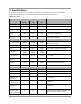
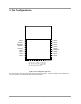
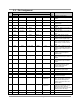
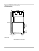
Table Of Contents
- 1. Introduction
- 2. Specifications
- 3. Pin Configurations
- 4. Electrical Characteristics
- Appendix A Additional Information
- A.1 Outline Drawing
- A.2 Module PCB Footprint
- A.3 Optimal PCB placement of the JN5168-001-M00 Module
- A.4 JN5168-001-M00 Antenna Radiation Pattern
- A.5 Manufacturing
- A.5.1 Reflow Profile
- A.5.2 Soldering Paste and Cleaning
- A.6 Ordering Information
- A.7 Related Documents
- A.8 Federal Communication Commission Interference Statement
- A.8.1 Antennas approved by FCC for use with JN5168 modules
- A.8.2 High Power Module usage limitation
- A.8.3 FCC End Product Labelling
- A.9 Industry Canada Statement
- A.9.1 Industry Canada End Product Labelling
- A.10 European R & TTE Directive 1999/5/EC Statement
- A.11 RoHS Compliance
- A.12 Status Information
- A.13 Disclaimers
- Version Control

4 JN-DS-JN5168-001-Myy 1v0 © NXP Laboratories UK 2012
2. Specifications
Most specification parameters for the modules are specified in the chip datasheet - JN-DS-JN5168 Wireless
Microcontroller Datasheet [2]. Where there are differences, the parameters are defined here.
VDD=3.0V @ +25°C
Typical DC Characteristics
Notes
JN5168-001-
M00/03
JN5168-001-
M06
JN5168-001-
M05
Deep sleep current
100nA
100nA
100nA
Sleep current
0.70uA
0.70uA
0.70uA
With active sleep timer
Radio transmit
current
15mA 175mA 35mA CPU in doze, radio transmitting
Radio receive
current
17.5mA 22mA 22mA CPU in doze, radio receiving
Centre frequency
accuracy
+/-25ppm +/-25ppm +/-25ppm
Additional +/-15ppm allowance for
temperature and ageing
Typical RF Characteristics
Notes
Receive sensitivity -95dBm -100dBm -96dBm
Nominal for 1% PER, as per 802.15.4
section 6.5.3.3 (Note 1)
Transmit power
2.5dBm
22dBm
9.5 dBm
Nominal
Maximum input
signal
10dBm 5dBm 10dBm For 1% PER, measured as sensitivity
RSSI range
-95 to
-10dBm
-105 to
-20dBm
-95 to
-10dBm
RF Port impedance
– uFL connector
50 ohm 50 ohm 50 ohm 2.4 - 2.5GHz
Rx Spurious
Emissions
-61dBm -69dBm -69dBm Measured conducted into 50ohms
Tx Spurious
Emissions
-40dBm -49dBm -45dBm Measured conducted into 50ohms
VSWR (max)
2:1
2:1
2:1
2.4 - 2.5GHz
Peripherals
Notes
Master SPI port
3 selects
3 selects
3 selects
250kHz - 16MHz
Slave SPI port
250kHz - 8MHz
Two UARTs
16550 compatible
Two-wire serial I/F
(compatible with
SMbus & I
2
C)
Up to 400kHz
5 x PWM (4 x timer,
1 x timer/counter)
16MHz clock
Two programmable
Sleep Timers
32kHz clock
Digital IO lines
(multiplexed with
UARTs, timers and
20 18 18
DIO2 & DIO3 not available on JN5168-001-
M05 and JN5168-001-M06 modules