
User's Guide


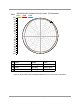


Table Of Contents
- 1. Introduction
- 2. Specifications
- 3. Pin Configurations
- 4. Electrical Characteristics
- Appendix A Additional Information
- A.1 Outline Drawing
- A.2 Module PCB Footprint
- A.3 Optimal PCB placement of the JN5168-001-M00 Module
- A.4 JN5168-001-M00 Antenna Radiation Pattern
- A.5 Manufacturing
- A.5.1 Reflow Profile
- A.5.2 Soldering Paste and Cleaning
- A.6 Ordering Information
- A.7 Related Documents
- A.8 Federal Communication Commission Interference Statement
- A.8.1 Antennas approved by FCC for use with JN5168 modules
- A.8.2 High Power Module usage limitation
- A.8.3 FCC End Product Labelling
- A.9 Industry Canada Statement
- A.9.1 Industry Canada End Product Labelling
- A.10 European R & TTE Directive 1999/5/EC Statement
- A.11 RoHS Compliance
- A.12 Status Information
- A.13 Disclaimers
- Version Control

24 JN-DS-JN5168-001-Myy 1v0 © NXP Laboratories UK 2012
Version Control
Version Notes
1.0 Initial release
NXP Laboratories UK Ltd
Furnival Street
Sheffield
S1 4QT
United Kingdom
Tel: +44 (0)114 281 2655
Fax: +44 (0) 114 281 2951
For the contact details of your local NXP office or distributor, refer to the NXP web site:
www.nxp.com/jennic