
User's Guide
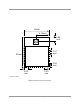
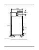


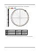

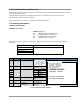

Table Of Contents
- 1. Introduction
- 2. Specifications
- 3. Pin Configurations
- 4. Electrical Characteristics
- Appendix A Additional Information
- A.1 Outline Drawing
- A.2 Module PCB Footprint
- A.3 Optimal PCB placement of the JN5168-001-M00 Module
- A.4 JN5168-001-M00 Antenna Radiation Pattern
- A.5 Manufacturing
- A.5.1 Reflow Profile
- A.5.2 Soldering Paste and Cleaning
- A.6 Ordering Information
- A.7 Related Documents
- A.8 Federal Communication Commission Interference Statement
- A.8.1 Antennas approved by FCC for use with JN5168 modules
- A.8.2 High Power Module usage limitation
- A.8.3 FCC End Product Labelling
- A.9 Industry Canada Statement
- A.9.1 Industry Canada End Product Labelling
- A.10 European R & TTE Directive 1999/5/EC Statement
- A.11 RoHS Compliance
- A.12 Status Information
- A.13 Disclaimers
- Version Control

© NXP Laboratories UK 2012 JN-DS-JN5168-001-Myy 1v0 19
A.5.2 Soldering Paste and Cleaning
NXP does not recommend use of a solder paste that requires the module and PCB assembly to be cleaned (rinsed in
water) for the following reasons:
Solder flux residues and water can be trapped by the PCB, can or components and result in short circuits.
The module label could be damaged or removed.
NXP recommends use of a 'no clean' solder paste for all its module products.
A.6 Ordering Information
Ordering Code Format:
Where this Data Sheet is denoted as “Advanced” or “Preliminary”, devices will be either Engineering Samples or
Prototypes.
Part Number Description
JN5168-001-M00 Shipped in tape mounted 500 piece reel
JN5168-001-M03
JN5168-001-M05
JN5168-001-M06
Line
Content
Format
Options
Sample
1
NXP Logo
B&W outline logo
JN5168-001-M00
ZSDYWW NNNNN
FCC ID:TYOJN5168M0
IC:7438A-CYO5168M0
2
Part ID
JN5168-001-M0x
x is module type, 0,
3, 5 or 6
3
Z
SSMC
S
APK
D
RoHs
Compliant
Y
Year
WW
Week
3
Serial No.
NNNNN
Serial number from
test
5
FCC ID
FCCID:TYOJN5168Mx
x is module type
0,3,5 or 6
6
IC ID
IC:7438A-
CYO5168Mx
x is module type
0,3,5 or 6
JN5168 - 001 – MYY
Module Type (YY)
00 Standard Power, Integral antenna
03 Standard Power, uFl connector
05 Medium Power, uFL connector
06 High Power, uFl connector
Figure 13: Example module labelling