
User's Guide
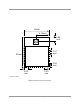
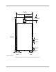


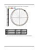

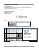

Table Of Contents
- 1. Introduction
- 2. Specifications
- 3. Pin Configurations
- 4. Electrical Characteristics
- Appendix A Additional Information
- A.1 Outline Drawing
- A.2 Module PCB Footprint
- A.3 Optimal PCB placement of the JN5168-001-M00 Module
- A.4 JN5168-001-M00 Antenna Radiation Pattern
- A.5 Manufacturing
- A.5.1 Reflow Profile
- A.5.2 Soldering Paste and Cleaning
- A.6 Ordering Information
- A.7 Related Documents
- A.8 Federal Communication Commission Interference Statement
- A.8.1 Antennas approved by FCC for use with JN5168 modules
- A.8.2 High Power Module usage limitation
- A.8.3 FCC End Product Labelling
- A.9 Industry Canada Statement
- A.9.1 Industry Canada End Product Labelling
- A.10 European R & TTE Directive 1999/5/EC Statement
- A.11 RoHS Compliance
- A.12 Status Information
- A.13 Disclaimers
- Version Control

18 JN-DS-JN5168-001-Myy 1v0 © NXP Laboratories UK 2012
Figure 11: Peak Field Strengths for various modules optimised for height and azimuth
A.5 Manufacturing
A.5.1 Reflow Profile
For reflow soldering, it is recommended to follow the reflow profile in figure 6 as a guide, as well as the paste
manufacturer’s guidelines on peak flow temperature, soak times, time above liquid and ramp rates.
Figure 12: Recommended solder reflow profile
98.0
98.5
99.0
99.5
100.0
100.5
101.0
101.5
102.0
102.5
103.0
103.5
104.0
11
18
26
dBuV/m @ 3m
Channel
Module Peak Field Strengths
JN5168-001-M03 with
vertical
JN5168-001-M00
JN5148-001-M00
Temperature 25~160 ºC 160~190 ºC > 220º C 230~Pk. Pk. Temp
(235ºC)
Target Time (s) 90~130 30~60 20~50 10~15 150~270