
User's Guide
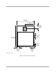
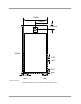


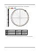

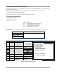

Table Of Contents
- 1. Introduction
- 2. Specifications
- 3. Pin Configurations
- 4. Electrical Characteristics
- Appendix A Additional Information
- A.1 Outline Drawing
- A.2 Module PCB Footprint
- A.3 Optimal PCB placement of the JN5168-001-M00 Module
- A.4 JN5168-001-M00 Antenna Radiation Pattern
- A.5 Manufacturing
- A.5.1 Reflow Profile
- A.5.2 Soldering Paste and Cleaning
- A.6 Ordering Information
- A.7 Related Documents
- A.8 Federal Communication Commission Interference Statement
- A.8.1 Antennas approved by FCC for use with JN5168 modules
- A.8.2 High Power Module usage limitation
- A.8.3 FCC End Product Labelling
- A.9 Industry Canada Statement
- A.9.1 Industry Canada End Product Labelling
- A.10 European R & TTE Directive 1999/5/EC Statement
- A.11 RoHS Compliance
- A.12 Status Information
- A.13 Disclaimers
- Version Control

14 JN-DS-JN5168-001-Myy 1v0 © NXP Laboratories UK 2012
A.3 Optimal PCB placement of the JN5168-001-M00 Module
The JN5168-001-M00 module features an optimised, low cost, integrated, inverted F, printed PCB antenna. The
antenna has a vertically polarised near omnidirectional radiation pattern and up to 1.6 dBi of peak gain. The PCB
design has been elongated in order to increase the ground plane area which increases the antenna efficiency. This
allows stand alone operation without any additional ground plane however care must be taken when mounting this
module onto another PCB. The area around the antenna must be kept clear of conductors or other metal objects for
an absolute minimum of 20 mm. This is true for all layers of the PCB and not just the top layer. Any conductive
objects close to the antenna could severely disrupt the antenna pattern resulting in deep nulls and high directivity in
some directions.
The diagrams below show various possible scenarios. The top 3 scenarios are correct; groundplane may be placed
beneath JN5168-001-M00 module as long as it does not protrude beyond the edge of the top layer ground plane on
the module PCB.
The bottom 3 scenarios are incorrect; the left hand side example because there is groundplane underneath the
antenna, the middle example because there is insufficient clearance around the antenna (it is best to have no
conductors anywhere near the antenna), finally the right hand example has a battery’s metal casing in the
recommended keep out area.
Figure 6 PCB placement of the JN5168-001-M00 Module