
User's Manual

Jennic
JennicJennic
Jennic
© Jennic 2009 JN-DS-JN5148-001-Myy 1v1 9
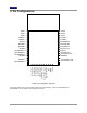
5. Electrical Characteristics
In most cases, the Electrical Characteristics are the same for both module and chip. They are described in detail in
the chip datasheet. Where there are differences, they are detailed below.
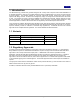
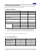
5.1. Maximum Ratings
Exceeding these conditions will result in damage to the device.
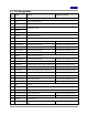
Parameter Min Max
Device supply voltage VDD -0.3V 3.6V
Voltage on analogue pins VREF, ADC1-4, DAC1-2,
COMP1M, COMP1P, COMP2M, COMP2P, IBIAS
-0.3V VDD + 0.3V
Voltage on 5v tolerant digital pins DIO0-DIO8 &
DIO11-20, RESETN
-0.3V Lower of (VDD + 2V) and
5.5V
Voltage on 3v tolerant digital pins DIO9, DIO10,
SPISSM, SPISWP, SPICLK, SPIMOSI, SPIMISO,
SPISSZ
-0.3V VDD + 0.3V
Storage temperature -40ºC 150ºC
Human Body Model
1
2.0kV
Machine Model
2
200V
ESD rating
Charged Device Model
3
500V
1) Testing for Human Body Model discharge is performed as specified in JEDEC Standard JESD22-A114.
2) Testing for Machine Model discharge is performed as specified in JEDEC Standard JESD11-A115.
3) Testing for Charged Device Model discharge is performed as specified in JEDEC Standard JESD22-C101.
This device is sensitive to ESD and should only be handled using ESD precautions.
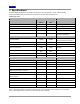
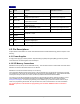
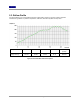
5.2. Operating Conditions
Supply Min Max
VDD (Module M00/M03) 2.3V 3.6V
VDD (Module M04) 2.7V 3.6V
Ambient temperature range
-40°C 85°C