
User's Manual

Jennic
JennicJennic
Jennic
ii JN-DS-JN5148-001-Myy 1v1 © Jennic 2009
Contents
1. Introduction 3
1.1. Variants 3
1.2. Regulatory Approvals 3
2. Specifications 4
3. Product Development 5
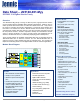
3.1. JN5148 Single Chip Wireless Microcontroller 5
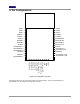
4. Pin Configurations 6
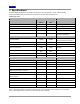
4.1. Pin Assignment 7
4.2. Pin Descriptions 8
4.2.1 Power Supplies 8
4.2.2 SPI Memory Connections 8
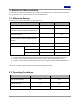
5. Electrical Characteristics 9
5.1. Maximum Ratings 9
5.2. Operating Conditions 9
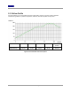
5.3. Reflow Profile 10
Appendix A Additional Information
11
A.1 Outline Drawing 11
A.2 Module PCB Footprint 14
A.3 Ordering Information 15
A.4 Tape and Reel Information: 16
A.4.1 Tape Orientation and dimensions 16
A.4.2 Cover tape details 16
A.4.3 Leader and Trailer 17
A.4.4 Reel Dimensions: 17
A.5 Related Documents 17
A.6 Federal Communication Commission Interference Statement 18
A.6.1 Antennas to be approved by FCC for use with JN5148 modules 19
A.6.2 High Power Module usage limitation 20
A.6.3 High Power Module channel restriction 20
A.6.4 FCC End Product Labelling 20
A.7 Industry Canada Statement 20
A.7.1 Industry Canada End Product Labelling 20
A.8 European R & TTE Directive 1999/5/EC Statement 20
A.9 RoHS Compliance 21
A.10 Status Information 21
A.11 Disclaimers 22
A.12 Version Control 23